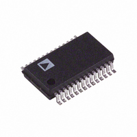
AD976ABRS Analog Devices Inc, AD976ABRS Datasheet - Page 4

AD976ABRS
Manufacturer Part Number
AD976ABRS
Description
IC ADC 16BIT 200KSPS 28-SSOP
Manufacturer
Analog Devices Inc
Datasheet
1.AD976ANZ.pdf
(16 pages)
Specifications of AD976ABRS
Rohs Status
RoHS non-compliant
Number Of Bits
16
Sampling Rate (per Second)
200k
Data Interface
Parallel
Number Of Converters
1
Power Dissipation (max)
100mW
Voltage Supply Source
Analog and Digital
Operating Temperature
-40°C ~ 85°C
Mounting Type
Surface Mount
Package / Case
28-SSOP (0.200", 5.30mm Width)
Number Of Elements
1
Resolution
16Bit
Architecture
SAR
Sample Rate
200KSPS
Input Polarity
Bipolar
Input Type
Voltage
Rated Input Volt
±10V
Differential Input
No
Power Supply Requirement
Analog and Digital
Single Supply Voltage (typ)
5V
Single Supply Voltage (min)
4.75V
Single Supply Voltage (max)
5.25V
Dual Supply Voltage (typ)
Not RequiredV
Dual Supply Voltage (min)
Not RequiredV
Dual Supply Voltage (max)
Not RequiredV
Power Dissipation
100mW
Differential Linearity Error
-1LSB/1.75LSB
Integral Nonlinearity Error
±2LSB
Operating Temp Range
-40C to 85C
Operating Temperature Classification
Industrial
Mounting
Surface Mount
Pin Count
28
Package Type
SSOP
Input Signal Type
Single-Ended
For Use With
EVAL-AD976CB - BOARD EVAL FOR AD976EVAL-AD976ACB - BOARD EVAL FOR AD976A
Lead Free Status / Rohs Status
Not Compliant
Available stocks
Company
Part Number
Manufacturer
Quantity
Price
Part Number:
AD976ABRS
Manufacturer:
ADI/亚德诺
Quantity:
20 000
Part Number:
AD976ABRSZ
Manufacturer:
ADI/亚德诺
Quantity:
20 000
TIMING SPECIFICATIONS
AD976/AD976A
Parameter
DIGITAL OUTPUTS
DIGITAL TIMING
POWER SUPPLIES
TEMPERATURE RANGE
Specifications subject to change without notice.
Convert Pulsewidth
Data Valid Delay after R/C Low (AD976A/AD976)
BUSY Delay from R/C Low
BUSY Low (AD976A/AD976)
BUSY Delay after End of Conversion (AD976A/AD976)
Aperture Delay
Conversion Time (AD976A/AD976)
Acquisition Time
Bus Relinquish Time
BUSY Delay after Data Valid (AD976A/AD976)
Previous Data Valid after R/C Low (AD976A/AD976)
Throughput Time (AD976A/AD976)
R/C to CS Setup Time
Time Between Conversions (AD976A/AD976)
Bus Access and Byte Delay
Specifications subject to change without notice.
Data Format
Data Coding
Leakage Current
Output Capacitance
Bus Access Time
Bus Relinquish Time
Specified Performance
Power Dissipation
Specified Performance
V
V
V
V
I
I
DIG
ANA
OL
OH
DIG
ANA
(AD976A: F
S
Conditions
I
I
High-Z State,
V
High-Z State
= 200 kHz; AD976: F
SINK
SOURCE
OUT
= 1.6 mA
= 0 V to V
= 500 A
–4–
DIG
Symbol
t
t
t
t
t
t
t
t
t
t
t
t
t
t
t
1
2
3
4
5
6
7
8
9
10
11
7
12
13
14
S
+ t
= 100 kHz; –40 C to +85 C, V
8
Min
+4
4.75
4.75
–40
Min
50
1.0/2.0
10
50
10
5/10
10
Binary Twos Complement
Parallel 16 Bits
All Grades
Typ
5
5
3.0
11
Typ
180/360
40
3.8/7.6
35
180/360
3.7/7.4
DIG
= V
ANA
= +5 V unless otherwise noted)
Max
+0.4
15
83
83
5.25
5.25
100
+85
Max
4.0/8.0
83
4.0/8.0
4.0/8.0
83
5/10
83
5
V
V
pF
V
V
mA
mA
mW
Units
ns
ns
REV. C
Units
ns
ns
ns
ns
ns
ns
ns
ns
C
A
s
s
s
s
s
s
s


