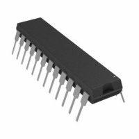
AD7713AN Analog Devices Inc, AD7713AN Datasheet - Page 9

AD7713AN
Manufacturer Part Number
AD7713AN
Description
IC ADC 24BIT SIGMA-DELTA 24-DIP
Manufacturer
Analog Devices Inc
Datasheet
1.AD7713ARZ.pdf
(28 pages)
Specifications of AD7713AN
Rohs Status
RoHS non-compliant
Number Of Bits
24
Sampling Rate (per Second)
205
Data Interface
Serial
Number Of Converters
1
Power Dissipation (max)
5.5mW
Voltage Supply Source
Analog and Digital
Operating Temperature
-40°C ~ 85°C
Mounting Type
Through Hole
Package / Case
24-DIP (0.300", 7.62mm)
CONTROL REGISTER (24 BITS)
A write to the device with the A0 input low writes data to the
control register. A read to the device with the A0 input low
accesses the contents of the control register. The control register
is 24 bits wide. When writing to the register, 24 bits of data
must be written; otherwise, the data will not be loaded to the
MD2
0
0
0
0
1
1
1
1
REV. D
Operating Mode
MD1
0
0
1
1
0
0
1
1
MSB
MD2
FS11
MD0
0
1
0
1
0
1
0
1
MD1
FS10
Operating Mode
Normal Mode. This is the normal mode of operation of the device whereby a read to the device with A0 high
accesses data from the data register. This is the default condition of these bits after the internal power-on reset.
Activate Self-Calibration. This activates self-calibration on the channel selected by CH0 and CH1. This is
a 1-step calibration sequence, and when complete, the part returns to normal mode (with MD2, MD1,
MD0 of the control registers returning to 0, 0, 0). The DRDY output indicates when this self-calibration
is complete. For this calibration type, the zero-scale calibration is done internally on shorted (zeroed)
inputs, and the full-scale calibration is done on V
Activate System Calibration. This activates system calibration on the channel selected by CH0 and CH1.
This is a 2-step calibration sequence, with the zero-scale calibration done first on the selected input
channel and DRDY indicating when this zero-scale calibration is complete. The part returns to normal
mode at the end of this first step in the 2-step sequence.
Activate System Calibration. This is the second step of the system calibration sequence with full-scale
calibration being performed on the selected input channel. Once again, DRDY indicates when the full-
scale calibration is complete. When this calibration is complete, the part returns to normal mode.
Activate System Offset Calibration. This activates system offset calibration on the channel selected by CH0
and CH1. This is a 1-step calibration sequence and, when complete, the part returns to normal mode with
DRDY indicating when this system offset calibration is complete. For this calibration type, the zero-scale
calibration is done on the selected input channel, and the full-scale calibration is done internally on V
Activate Background Calibration. This activates background calibration on the channel selected by CH0 and
CH1. If the background calibration mode is on, the AD7713 provides continuous self-calibration of the refer-
ence and shorted (zeroed) inputs. This calibration takes place as part of the conversion sequence, extending
the conversion time and reducing the word rate by a factor of 6. Its major advantage is that the user does
not have to worry about recalibrating the device when there is a change in the ambient temperature. In
this mode, the shorted (zeroed) inputs and V
monitored, and the calibration registers of the device are updated.
Read/Write Zero-Scale Calibration Coefficients. A read to the device with A0 high accesses the contents of
the zero-scale calibration coefficients of the channel selected by CH0 and CH1. A write to the device with
A0 high writes data to the zero-scale calibration coefficients of the channel selected by CH0 and CH1.
The word length for reading and writing these coefficients is 24 bits, regardless of the status of the WL bit
of the control register. Therefore, when writing to the calibration register, 24 bits of data must be written;
otherwise, the new data will not be transferred to the calibration register.
Read/Write Full-Scale Calibration Coefficients. A read to the device with A0 high accesses the contents of
the full-scale calibration coefficients of the channel selected by CH0 and CH1. A write to the device with
A0 high writes data to the full-scale calibration coefficients of the channel selected by CH0 and CH1. The
word length for reading and writing these coefficients is 24 bits, regardless of the status of the WL bit of
the control register. Therefore, when writing to the calibration register, 24 bits of data must be written;
otherwise, the new data will not be transferred to the calibration register.
MD0
FS9
G2
FS8
G1
FS7
G0
FS6
–9–
CH1
FS5
control register. In other words, it is not possible to write just
the first 12 bits of data into the control register. If more than 24
clock pulses are provided before TFS returns high, then all clock
pulses after the 24th clock pulse are ignored. Similarly, a read
operation from the control register should access 24 bits of data.
REF
CH0
FS4
, as well as the analog input voltage, are continuously
REF
.
WL
FS3
RO
FS2
BO
FS1
B/U
FS0
LSB
AD7713
REF
.


