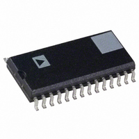
AD976ARZ Analog Devices Inc, AD976ARZ Datasheet - Page 6

AD976ARZ
Manufacturer Part Number
AD976ARZ
Description
IC ADC 16BIT 100KSPS 28-SOIC
Manufacturer
Analog Devices Inc
Datasheet
1.AD976ANZ.pdf
(16 pages)
Specifications of AD976ARZ
Data Interface
Parallel
Number Of Bits
16
Sampling Rate (per Second)
200k
Number Of Converters
1
Power Dissipation (max)
100mW
Voltage Supply Source
Analog and Digital
Operating Temperature
-40°C ~ 85°C
Mounting Type
Surface Mount
Package / Case
28-SOIC (0.300", 7.50mm Width)
Resolution (bits)
16bit
Sampling Rate
100kSPS
Input Channel Type
Single Ended
Supply Voltage Range - Analog
4.75V To 5.25V
Supply Voltage Range - Digital
4.75V To 5.25V
Number Of Elements
1
Resolution
16Bit
Architecture
SAR
Sample Rate
100KSPS
Input Polarity
Bipolar
Input Type
Voltage
Rated Input Volt
±10V
Differential Input
No
Power Supply Requirement
Analog and Digital
Single Supply Voltage (typ)
5V
Single Supply Voltage (min)
4.75V
Single Supply Voltage (max)
5.25V
Dual Supply Voltage (typ)
Not RequiredV
Dual Supply Voltage (min)
Not RequiredV
Dual Supply Voltage (max)
Not RequiredV
Power Dissipation
100mW
Differential Linearity Error
-2LSB/3LSB
Integral Nonlinearity Error
±3LSB
Operating Temp Range
-40C to 85C
Operating Temperature Classification
Industrial
Mounting
Surface Mount
Pin Count
28
Package Type
SOIC W
Input Signal Type
Single-Ended
Lead Free Status / RoHS Status
Lead free / RoHS Compliant
For Use With
EVAL-AD976CB - BOARD EVAL FOR AD976EVAL-AD976ACB - BOARD EVAL FOR AD976A
Lead Free Status / Rohs Status
Compliant
Available stocks
Company
Part Number
Manufacturer
Quantity
Price
Part Number:
AD976ARZ
Manufacturer:
ADI/亚德诺
Quantity:
20 000
Company:
Part Number:
AD976ARZRL
Manufacturer:
ADI
Quantity:
25
DEFINITION OF SPECIFICATIONS
INTEGRAL NONLINEARITY ERROR (INL)
Linearity error refers to the deviation of each individual code
from a line drawn from “negative full scale” to “positive full
scale.” The point used as negative full scale occurs 1/2 LSB
before the first code transition. Positive full scale is defined as a
level 1 1/2 LSB beyond the last code transition. The deviation is
measured from the middle of each particular code to the true
straight line.
DIFFERENTIAL NONLINEARITY ERROR (DNL)
In an ideal ADC, code transitions are 1 LSB apart. Differential
nonlinearity is the maximum deviation from this ideal value. It
is often specified in terms of resolution for which no missing
codes are guaranteed.
The last + transition (from 011. . .10 to 011. . .11) should
occur for an analog voltage 1 1/2 LSB below the nominal full
scale (9.9995422 V for a 10 V range). The full-scale error is
the deviation of the actual level of the last transition from the
ideal level.
AD976/AD976A
Pin No.
1
2
3
4
5
6
7–13
14
15–21
22
23
24
25
26
27
28
FULL-SCALE ERROR
Mnemonic
V
AGND1
REF
CAP
AGND2
D15 (MSB)
D14–D8
DGND
D7–D1
D0 (LSB)
BYTE
R/C
CS
BUSY
V
V
IN
ANA
DIG
Description
Analog Input. Connect a 200
input range is 10 V.
Analog Ground. Used as the ground reference point for the REF pin.
Reference Input/Output. The internal +2.5 V reference is available at this pin. Alternatively, an
external reference can be used to override the internal reference. In either case, connect a 2.2 F
tantalum capacitor between REF and AGND1.
Reference Buffer Output. Connect a 2.2 F tantalum capacitor between CAP and AGND2.
Analog Ground.
Data Bit 15. Most significant bit of conversion result. High impedance state when CS is HIGH or
when R/C is LOW.
Data Bits 14–8. High impedance state when CS is HIGH or when R/C is LOW.
Digital Ground.
Data Bits 7–1. High impedance state when CS is HIGH or when R/C is LOW.
Data Bit 0. Least significant bit of conversion result. High impedance state when CS is HIGH or
when R/C is LOW.
Byte Select. With BYTE LOW, data will be output as indicated above; Pin 6 (D15) is the MSB,
Pin 22 (D0) is the LSB. With BYTE HIGH, the top and bottom 8 bits of data will be switched;
D15–D8 are output on Pins 15–22 and D7–D0 are output on Pins 6–13.
Read/Convert Input. With CS LOW, a falling edge on R/C puts the internal sample/hold into the
hold state and starts a conversion; a rising edge enables the output data bits.
Chip Select Input. Internally OR’d with R/C. With R/C LOW, a falling edge on CS will initiate a
conversion. With R/C HIGH, a falling edge on CS will enable the output data bits. When CS is
HIGH, the output data bits will be in the Hi-impedance state.
Busy Output. Goes LOW when a conversion is started and remains LOW until the conversion is
completed and the data is latched into the output register. With CS tied LOW and R/C HIGH,
output data will be valid when BUSY rises. The rising edge of BUSY can be used to latch the out-
put data.
Analog Power Supply. Nominally +5 V.
Digital Power Supply. Nominally +5 V.
PIN FUNCTION DESCRIPTIONS
–6–
resistor between V
BIPOLAR ZERO ERROR
Bipolar zero error is the difference between the ideal midscale
input voltage (0 V) and the actual voltage producing the midscale
output code.
INPUT BANDWIDTH
The input bandwidth is that frequency at which the amplitude
of the reconstructed fundamental is reduced by 3 dB for a full-
scale input.
FULL-POWER BANDWIDTH
Full-power bandwidth is defined as the full-scale input fre-
quency at which signal to (Noise + Distortion) degrades to
60 dB, as 10 bits of accuracy.
APERTURE DELAY
Aperture delay is a measure of the Sample-and-Hold Amplifier
(SHA) performance and is measured from the rising edge of the
clock input to when the input signal is held for a conversion.
IN
and the analog signal source. The full-scale
REV. C


