AD7861AP Analog Devices Inc, AD7861AP Datasheet - Page 6
AD7861AP
Manufacturer Part Number
AD7861AP
Description
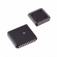
IC ADC 11BIT 4CH 44-PLCC
Manufacturer
Analog Devices Inc
Datasheet
1.AD7861APZ.pdf
(6 pages)
Specifications of AD7861AP
Rohs Status
RoHS non-compliant
Number Of Bits
11
Sampling Rate (per Second)
28.6k
Data Interface
Parallel
Number Of Converters
1
Power Dissipation (max)
50mW
Voltage Supply Source
Single Supply
Operating Temperature
-40°C ~ 85°C
Mounting Type
Surface Mount
Package / Case
44-PLCC
Available stocks
Company
Part Number
Manufacturer
Quantity
Price
Company:

Part Number:
AD7861AP
Manufacturer:
Analog Devices Inc.
Quantity:
245
Part Number:
AD7861AP
Manufacturer:
ADI/亚德诺
Quantity:
20 000
Company:
Part Number:
AD7861APZ
Manufacturer:
Analog Devices Inc
Quantity:
10 000


AD7861
DESCRIPTION OF THE REGISTERS
VIN1, VIN2, VIN3
AUX
Reading Results
The A/D conversion results for channels VIN1, VIN2, VIN3
and AUX are stored in the VIN1, VIN2, VIN3 and AUX
registers respectively. The twos complement data is left justified
and the LSB (Data Bit 0) is set to zero. The relationship
between input voltage and output coding is shown in Figure 4.
Power Supply Connections and Setup
The nominal power supply level (V
positive power supply (V
and 36. The SGND and DGND pins should be star point
connected to AGND at a point close to the AD7861.
Power supplies should be bypassed at the power pins using a
0.1 µF capacitor. A 200 nF capacitor should also be connected
between REFIN and SGND.
0 1 1 1 1 1 1 1 1 1 1 0
0 0 0 0 0 0 0 0 0 0 0 0
1 0 0 0 0 0 0 0 0 0 0 0
Figure 4. AD7861 Transfer Function
These registers contain the results from
the conversion of the analog input voltages.
In the AD7861, this register contains the
conversion result of the auxiliary channel
which had been selected by S0, S1.
OUTPUT
CODE
0V
DD
) should be connected to Pins 21
INPUT VOLTAGE
2.5
DD
FULL-SCALE
TRANSITION
0.048 (1.21)
0.042 (1.07)
) is +5 V ± 5%. The
(0.50)
0.020
FS = 5V
LSB =
R
5V-1LSB
44-Lead Plastic Leadless Chip Carrier
2048
17
7
5V
18
6
Dimensions shown in inches and (mm).
0.048 (1.21)
0.042 (1.07)
0.656 (16.66)
0.650 (16.51) SQ
OUTLINE DIMENSIONS
0.695 (17.65)
0.685 (17.40) SQ
(PINS DOWN)
TOP VIEW
IDENTIFIER
PIN 1
0.056 (1.42)
0.042 (1.07)
(P-44A)
–6–
40
28
39
29
DIGITAL SIGNAL PROCESSOR INTERFACING
The AD7861 A/D converter is designed to be easily interfaced
to Analog Devices’ family of Digital Signal Processors (DSPs).
Figure 5 shows the interface between the AD7861 and the
ADSP-2101/2105/2115 16-bit fixed point DSP, and the ADSP-
2171 and ADSP-2181 DSP Microcomputers. FLAGOUT from
the DSP is used to initiate the AD7861 conversion and is also
used in conjunction with the BUSY signal to provide an end of
conversion interrupt for the DSP. With M0 and M1 tied low,
the AD7861 is set up in the VIN2, VIN3 channel conversion
mode. By mapping the 12-bit AD7861 data bus into the top 12
bits of the DSP data bus (D12–D23), full-scale outputs from the
AD7861 can be represented as ± 1.0 in fixed point arithmetic.
The AD7861 can operate with a clock frequency in the range of
6.25 MHz to 12.5 MHz. For the ADSP-2101/2105/2115 the
CLKOUT frequency is the system clock frequency. In the case
of the ADSP-2171/2181, the system clock is internally scaled, a
10 MHz system clock will result in a 20 MHz CLKOUT
frequency. If CLKOUT from the ADSP-2171/2181 is above
12.5 MHz, then an external clock divide down circuit will be
necessary.
Figure 5. ADI Digital Signal Processor/Microcomputer
Interface
0.180 (4.57)
0.165 (4.19)
ADSP-2101/
ADSP-2105/
ADSP-2115–12MHz
ADSP-2171–10MHz
ADSP-2181–10MHz
0.110 (2.79)
0.085 (2.16)
A0–A13
D0–D23
0.032 (0.81)
0.026 (0.66)
0.050
(1.27)
BSC
0.021 (0.53)
0.013 (0.33)
0.025 (0.63)
0.015 (0.38)
0.040 (1.01)
0.025 (0.64)
0.63 (16.00)
0.59 (14.99)
FLAGOUT
CLKOUT
IRQ2
DMS
RD
ADDRESS BUS
DATA BUS
ADDRESS
EN
DECODE
CLK
M0
M1
CS
BUSY
CONVST
RD
D0–D11*
A0–A1
AD7861
REV. B
Related parts for AD7861AP
Image
Part Number
Description
Manufacturer
Datasheet
Request
R

Part Number:
Description:
±1.7g Dual-Axis IMEMS Accelerometer Evaluation Board
Manufacturer:
Analog Devices Inc
Datasheet:

Part Number:
Description:
Inertial Sensor Evaluation System
Manufacturer:
Analog Devices Inc
Datasheet:
Part Number:
Description:
Manufacturer:
Analog Devices Inc
Datasheet:
Part Number:
Description:
Manufacturer:
Analog Devices Inc
Datasheet:
Part Number:
Description:
Manufacturer:
Analog Devices Inc
Datasheet:
Part Number:
Description:
Manufacturer:
Analog Devices Inc
Datasheet:
Part Number:
Description:
Manufacturer:
Analog Devices Inc
Datasheet:
Part Number:
Description:
Manufacturer:
Analog Devices Inc
Datasheet:
Part Number:
Description:
Manufacturer:
Analog Devices Inc
Datasheet:
Part Number:
Description:
Manufacturer:
Analog Devices Inc
Datasheet:
Part Number:
Description:
Manufacturer:
Analog Devices Inc
Datasheet:
Part Number:
Description:
Manufacturer:
Analog Devices Inc
Datasheet:
Part Number:
Description:
Manufacturer:
Analog Devices Inc
Datasheet: