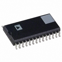
AD7721AR Analog Devices Inc, AD7721AR Datasheet - Page 12

AD7721AR
Manufacturer Part Number
AD7721AR
Description
IC ADC 16BIT SIGMA-DELTA 28-SOIC
Manufacturer
Analog Devices Inc
Datasheet
1.AD7721ARZ-REEL.pdf
(16 pages)
Specifications of AD7721AR
Rohs Status
RoHS non-compliant
Number Of Bits
16
Sampling Rate (per Second)
468.75k
Data Interface
Serial, Parallel
Number Of Converters
1
Power Dissipation (max)
150mW
Voltage Supply Source
Analog and Digital
Operating Temperature
-40°C ~ 85°C
Mounting Type
Surface Mount
Package / Case
28-SOIC (0.300", 7.50mm Width)
Available stocks
Company
Part Number
Manufacturer
Quantity
Price
Part Number:
AD7721AR
Manufacturer:
ADI/亚德诺
Quantity:
20 000
Part Number:
AD7721ARZ
Manufacturer:
ADI/亚德诺
Quantity:
20 000
AD7721
PARALLEL INTERFACE
Read Operation
The device defaults to parallel mode if CS, RD and WR are not
tied to DGND together. Figure 11 shows a timing diagram for
reading from the AD7721 in the parallel mode. When operating
the device in parallel mode, CS and RD should be tied to
DGND permanently except when control information is being
written to the AD7721. DRDY goes high for 2 clock cycles to
indicate that new data is available from the interface. The
AD7721 outputs this data after the falling edge of DRDY. This
DRDY pin can be used to drive an edge-triggered interrupt of a
microprocessor.
RFS (I) / DRDY (O)
NOTE: (I) SIGNIFIES AN INPUT; (O) SIGNIFIES AN OUTPUT.
DATA OUT (O)
SCLK (O)
DB0–DB11 (O)
DB0–DB11 (I)
NOTE: (I) SIGNIFIES AN INPUT; (O) SIGNIFIES AN OUTPUT.
NOTE: (I) SIGNIFIES AN INPUT; (O) SIGNIFIES AN OUTPUT.
DRDY (O)
WR (I)
CS (I)
CS (I)
RD (I)
t
1
t
3
t
2
DB15
Figure 11. Parallel Mode Output Register Read
Figure 10. Serial Mode Output Register Read
DB14
Figure 12. Write Timing Diagram
DB13
t
10
t
4
t
DB12
t
11
5
–12–
DB11
t
12
Write Operation
The write operation is used to write data into the control regis-
ter. The outputs of the control register select the analog input
range, allow the part to be put into power-down (standby)
mode, define the function of the DVAL/SYNC pin, and initiate
the calibration routine. After power-up and after at least 16
clock cycles, the control register must be written to. A cali-
bration must also be performed at least once after power-up to
set the calibration registers. The function of each bit in the
control register is shown in Table I. When writing to the con-
trol register, the RD pin must be taken high so that the pins D0
to D11 are configured as inputs.
t
9
DB10
t
6
VALID DATA
t
13
t
14
DB0
t
15
t
7
REV. A
t
8


