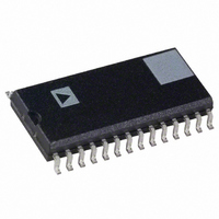
AD7719BR-REEL Analog Devices Inc, AD7719BR-REEL Datasheet - Page 27

AD7719BR-REEL
Manufacturer Part Number
AD7719BR-REEL
Description
IC ADC 16BIT 24BIT DUAL 28-SOIC
Manufacturer
Analog Devices Inc
Datasheet
1.AD7719BRUZ-REEL.pdf
(40 pages)
Specifications of AD7719BR-REEL
Rohs Status
RoHS non-compliant
Number Of Bits
16/24
Sampling Rate (per Second)
105
Data Interface
DSP, MICROWIRE™, QSPI™, Serial, SPI™
Number Of Converters
2
Power Dissipation (max)
4.5mW
Voltage Supply Source
Analog and Digital
Operating Temperature
-40°C ~ 85°C
Mounting Type
Surface Mount
Package / Case
28-SOIC (0.300", 7.50mm Width)
For Use With
EVAL-AD7719EB - BOARD EVAL FOR AD7719
REV. A
CONFIGURING THE AD7719
All user-accessible registers on the AD7719 are accessed via the
serial interface. Communication with any of these registers is
initiated by first writing to the Communications register.
Figure 11 outlines a flow diagram of the sequence used to con-
figure all registers after a power-up or reset on the AD7719. The
flowchart shows two methods of determining when it is valid to
read the data register or determine when a calibration cycle is
complete. The first method is hardware polling of the RDY
pin and the second method involves software interrogation of
bits in the status and mode registers. The flowchart details all the
necessary programming steps required to initialize the ADC and
read data from the main and aux channel following a power-on or
reset. The steps can be broken down as follows:
1. Configure and initialize the microcontroller or microprocessor
2. Initialize the AD7719 by configuring the following registers:
3. When the operating mode is selected, the user needs to deter-
serial port.
a) IOCON to configure the current sources and digital
b) FILTER to configure the update rate for both channels.
c) AD1CON to enable the aux channel, select the analog
d) AD0CON to enable the main ADC channel and select
e) MODE to configure the operating mode. Operating mode
All of these operations consist of a write to the communications
register to specify the next operation as a write to a specified
register. Data is then written to this register. When each
sequence is complete, the ADC defaults to waiting for
another write to the Communications register to specify the
next operation.
mine when it is valid to read the data in conversion mode or
when the calibration is complete in calibration mode. This is
accomplished either by polling the RDY pin (hardware polling)
or by interrogating the bits in either the Status or Mode
registers (software polling). Both are shown in Figure 11. It is
assumed that both the main and aux ADCs are being used
and calibration is required. If the AD7719 is operated at
the factory-calibrated conditions, a field calibration will not be
required and these steps can be bypassed.
I/O port.
input, select unipolar or bipolar operation and input range.
16-/24-bit mode, analog input range, and either unipolar
or bipolar operation.
consists of calibration or conversion.
–27–
MICROCOMPUTER/MICROPROCESSOR INTERFACING
The AD7719’s flexible serial interface allows for easy interface
to most microcomputers and microprocessors. The flowchart of
Figure 11 outlines the sequence that should be followed when
interfacing a microcontroller or microprocessor to the AD7719.
Figures 12, 13, and 14 show some typical interface circuits.
The serial interface on the AD7719 is capable of operating from
just three wires and is compatible with SPI interface protocols.
The 3-wire operation makes the part ideal for isolated systems
where minimizing the number of interface lines minimizes the
number of opto-isolators required in the system. The serial
clock input is a Schmitt-triggered input to accommodate slow
edges from optocouplers. The rise and fall times of other digital
inputs to the AD7719 should be no longer than 1 µs.
Most of the registers on the AD7719 are 8-bit registers, which
facilitates easy interfacing to the 8-bit serial ports of microcon-
trollers. The main channel data register (AD0) on the AD7719
can be either 16 or 24 bits, the aux ADC data register (AD1) is
16 bits wide and the offset and gain registers are 24-bit registers,
but data transfers to these registers can consist of multiple 8-bit
transfers to the serial port of the microcontroller. DSP proces-
sors and microprocessors generally transfer 16 bits of data in a
serial data operation. Some of these processors, such as the
ADSP-2105, have the facility to program the amount of cycles
in a serial transfer. This allows the user to tailor the number of
bits in any transfer to match the register length of the required
register in the AD7719.
Even though some of the registers on the AD7719 are only eight
bits in length, communicating with two of these registers in
successive write operations can be handled as a single 16-bit
data transfer, if required. For example, if the Filter register is to
be updated, the processor must first write to the Communica-
tions register (saying that the next operation is a write to the
Filter register) and then write eight bits to the Setup register. If
required, this can all be done in a single 16-bit transfer because
once the eight serial clocks of the write operation to the Com-
munications register have been completed, the part immediately
sets itself up for a write operation to the Setup register.
AD7719


