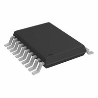
AD7998BRUZ-0 Analog Devices Inc, AD7998BRUZ-0 Datasheet - Page 24

AD7998BRUZ-0
Manufacturer Part Number
AD7998BRUZ-0
Description
IC ADC 12BIT 8CHAN I2C 20TSSOP
Manufacturer
Analog Devices Inc
Datasheet
1.AD7997BRUZ-1.pdf
(32 pages)
Specifications of AD7998BRUZ-0
Data Interface
I²C, Serial
Number Of Bits
12
Sampling Rate (per Second)
188k
Number Of Converters
1
Power Dissipation (max)
2.2mW
Voltage Supply Source
Single Supply
Operating Temperature
-40°C ~ 85°C
Mounting Type
Surface Mount
Package / Case
20-TSSOP (0.173", 4.40mm Width)
Resolution (bits)
12bit
Sampling Rate
188kSPS
Input Channel Type
Single Ended
Supply Voltage Range - Analog
2.7V To 5.5V
Supply Current
1.4mA
Lead Free Status / RoHS Status
Lead free / RoHS Compliant
For Use With
EVAL-AD7998CBZ - BOARD EVALUATION FOR AD7998CBZ
Lead Free Status / RoHS Status
Lead free / RoHS Compliant, Lead free / RoHS Compliant
Available stocks
Company
Part Number
Manufacturer
Quantity
Price
Part Number:
AD7998BRUZ-0
Manufacturer:
ADI/亚德诺
Quantity:
20 000
AD7997/AD7998
WRITING TO THE AD7997/AD7998
Depending on the register being written to, there are three
different writes for the AD7997/AD7998.
WRITING TO THE ADDRESS POINTER REGISTER
FOR A SUBSEQUENT READ
In order to read from a particular register, the address pointer
register must first contain the address of that register. If it does
not, the correct address must be written to the address pointer
register by performing a single-byte write operation, as shown
in Figure 26. The write operation consists of the serial bus
address followed by the address pointer byte. No data is written
to any of the data registers. A read operation may be subsequently
performed to read the register of interest.
WRITING A SINGLE BYTE OF DATA TO THE ALERT
STATUS REGISTER OR CYCLE REGISTER
The alert status register and cycle register are both 8-bit registers,
so only one byte of data can be written to each. Writing a single
byte of data to one of these registers consists of the serial bus
write address, the chosen data register address written to the
address pointer register, followed by the data byte written to the
selected data register. See Figure 27.
SDA
SCL
SDA
SCL
START BY
MASTER
START BY
MASTER
0
1
0
1
Figure 26. Writing to the Address Pointer Register to Select a Register for a Subsequent Read Operation
1
1
SERIAL BUS ADDRESS BYTE
SERIAL BUS ADDRESS BYTE
0
0
FRAME 1
A3
A3
FRAME 1
SCL (CONTINUED)
SDA (CONTINUED)
A2
A2
A1
A1
A0
A0
Figure 27. Single-Byte Write Sequence
R/W
R/W
AD7997/AD7998
AD7997/AD7998
ACK. BY
Rev. 0 | Page 24 of 32
ACK. BY
9
9
9
C4
C4
D7
1
1
1
C3
C3
D6
WRITING TWO BYTES OF DATA TO A LIMIT,
HYSTERESIS, OR CONFIGURATION REGISTER
Each of the four limit registers are 16-bit registers, so two bytes
of data are required to write a value to any one of them. Writing
two bytes of data to one of these registers consists of the serial
bus write address, the chosen limit register address written to
the address pointer register, followed by two data bytes written
to the selected data register. See Figure 28.
If the master is write addressing the AD7997/AD7998, it can
write to more than one register without readdressing the ADC.
After the first write operation has completed for the first data
register, during the next byte the master simply writes to the
address pointer byte to select the next data register for a write
operation. This eliminates the need to readdress the device in
order to write to another data register.
ADDRESS POINTER REGISTER BYTE
ADDRESS POINTER REGISTER BYTE
C2
C2
D5
C1
C1
D4
FRAME 2
DATA BYTE
FRAME 2
FRAME 3
P3
P3
D3
P2
P2
D2
P1
P1
D1
AD7997/AD7998
P0
AD7997/AD7998
P0
D0
AD7997/AD7998
ACK. BY
ACK. BY
ACK. BY
9
9
9
STOP BY
MASTER
STOP BY
MASTER


