LTC2208CUP Linear Technology, LTC2208CUP Datasheet - Page 20
LTC2208CUP
Manufacturer Part Number
LTC2208CUP
Description
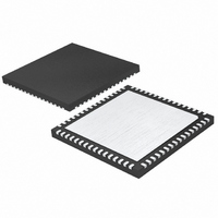
IC ADC 16BIT 130MSPS 64-QFN
Manufacturer
Linear Technology
Datasheet
1.LTC2208CUPPBF.pdf
(32 pages)
Specifications of LTC2208CUP
Number Of Bits
16
Sampling Rate (per Second)
130M
Data Interface
Parallel
Number Of Converters
1
Power Dissipation (max)
1.78W
Voltage Supply Source
Single Supply
Operating Temperature
0°C ~ 70°C
Mounting Type
Surface Mount
Package / Case
64-WFQFN, Exposed Pad
Lead Free Status / RoHS Status
Contains lead / RoHS non-compliant
Available stocks
Company
Part Number
Manufacturer
Quantity
Price

Part Number:
LTC2208CUP
Manufacturer:
LTNEAR
Quantity:
20 000
Part Number:
LTC2208CUP#PBF
Manufacturer:
LT/凌特
Quantity:
20 000
Company:
Part Number:
LTC2208CUP#TRPBF
Manufacturer:
ST
Quantity:
2 144


LTC2208
Figure 4a shows transformer coupling using a transmis-
sion line balun transformer. This type of transformer has
much better high frequency response and balance than
fl ux coupled center tap transformers. Coupling capacitors
are added at the ground and input primary terminals to
allow the secondary terminals to be biased at 1.25V. Figure
4b shows the same circuit with components suitable for
higher input frequencies.
ANALOG
Direct Coupled Circuits
Figure 5 demonstrates the use of a differential amplifi er to
convert a single ended input signal into a differential input
signal. The advantage of this method is that it provides
low frequency input response; however, the limited gain
bandwidth of any op amp or closed-loop amplifi er will de-
grade the ADC SFDR at high input frequencies. Additionally,
wideband op amps or differential amplifi ers tend to have
high noise. As a result, the SNR will be degraded unless
the noise bandwidth is limited prior to the ADC input.
APPLICATIONS INFORMATION
20
ANALOG
INPUT
Figure 4a. Using a Transmission Line Balun Transformer.
Recommended for Input Frequencies from 100MHz to 250MHz
INPUT
Figure 4b. Using a Transmission Line Balun Transformer.
Recommended for Input Frequencies from 250MHz to 500MHz
0.1μF
0.1μF
0.1μF
0.1μF
T1 = MA/COM ETC1-1-13
RESISTORS, CAPACITORS
ARE 0402 PACKAGE SIZE
EXCEPT 2.2μF
T1 = MA/COM ETC1-1-13
RESISTORS, CAPACITORS
ARE 0402 PACKAGE SIZE
EXCEPT 2.2μF
1:1
1:1
T1
T1
25Ω
25Ω
25Ω
25Ω
0.1μF
0.1μF
10Ω
10Ω
4.7pF
2.2μF
2.2pF
2.2pF
5Ω
5Ω
2.2μF
4.7pF
4.7pF
5Ω
5Ω
V
V
A
A
A
A
CM
IN
IN
CM
IN
IN
+
–
+
–
LTC2208
LTC2208
2208 F04a
2208 F04b
Reference Operation
Figure 6 shows the LTC2208 reference circuitry consisting
of a 2.5V bandgap reference, a programmable gain ampli-
fi er and control circuit. The LTC2208 has three modes of
reference operation: Internal Reference, 1.25V external
reference or 2.5V external reference. To use the internal
reference, tie the SENSE pin to V
reference, simply apply either a 1.25V or 2.5V reference
voltage to the SENSE input pin. Both 1.25V and 2.5V applied
to SENSE will result in a full scale range of 2.25V
= 0). A 1.25V output, V
bias for input drive circuitry. An external bypass capacitor is
required for the V
low impedance path to ground for internal and external
circuitry. This is also the compensation capacitor for the
reference; it will not be stable without this capacitor. The
minimum value required for stability is 2.2μF .
TIE TO V
EXTERNAL 1.25V
EXTERNAL 2.5V
INTERNAL 2.5V
OR INPUT FOR
OR INPUT FOR
ANALOG
REFERENCE
INPUT
Figure 5. DC-Coupled Input with Differential Amplifi er
REFERENCE
REFERENCE
DD
TO USE
AMPLIFIER = LTC6600-20,
LTC1993, ETC.
SENSE
DIFFERENTIAL
+
CM
–
2.2μF
V
HIGH SPEED
AMPLIFIER
CM
Figure 6. Reference Circuit
CM
+
–
output. This provides a high frequency
CM
BUFFER
is provided for a common mode
25Ω
25Ω
AND GAIN
CONTROL
SELECT
RANGE
2.2μF
DD
12pF
12pF
1.25V
. To use an external
V
A
A
CM
IN
IN
+
–
PGA
LTC2208
REFERENCE
BANDGAP
REFERENCE
P-P
INTERNAL
2.5V
2208 F05
ADC
(PGA
2208 F06
2208fc
Related parts for LTC2208CUP
Image
Part Number
Description
Manufacturer
Datasheet
Request
R

Part Number:
Description:
CD ROM LINEARVIEW DATASHEETS
Manufacturer:
Linear Technology

Part Number:
Description:
Standalone Linear Li-Ion Battery Charger with Thermal Regulation in ThinSOT
Manufacturer:
Linear Technology Corporation
Datasheet:
Part Number:
Description:
Low noise, high frequency, 8th order linear phase lowpass filter
Manufacturer:
Linear Technology Corporation
Datasheet:
Part Number:
Description:
Manufacturer:
Linear Technology Corporation
Datasheet:
Part Number:
Description:
Manufacturer:
Linear Technology Corporation
Datasheet:
Part Number:
Description:
Manufacturer:
Linear Technology Corporation
Datasheet:
Part Number:
Description:
Manufacturer:
Linear Technology Corporation
Datasheet:
Part Number:
Description:
Manufacturer:
Linear Technology Corporation
Datasheet:
Part Number:
Description:
Manufacturer:
Linear Technology Corporation
Datasheet:
Part Number:
Description:
Manufacturer:
Linear Technology Corporation
Datasheet:
Part Number:
Description:
Dual and Quad, JFET Input Precision High Speed Op Amps
Manufacturer:
Linear Technology Corporation
Datasheet:
Part Number:
Description:
Manufacturer:
Linear Technology Corporation
Datasheet:
Part Number:
Description:
1, 2, 6 and 8 Channel, 10-Bit Serial I/O Data Acquisition Systems
Manufacturer:
Linear Technology Corporation
Datasheet:
Part Number:
Description:
Manufacturer:
Linear Technology Corporation
Datasheet:
Part Number:
Description:
Universal dual filter building block
Manufacturer:
Linear Technology Corporation
Datasheet: