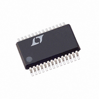
LTC2408CG#TRPBF Linear Technology, LTC2408CG#TRPBF Datasheet - Page 24

LTC2408CG#TRPBF
Manufacturer Part Number
LTC2408CG#TRPBF
Description
IC A/D CONV 24BIT 8-CHAN 28-SSOP
Manufacturer
Linear Technology
Datasheet
1.LTC2408CGPBF.pdf
(36 pages)
Specifications of LTC2408CG#TRPBF
Number Of Bits
24
Sampling Rate (per Second)
7.5
Data Interface
MICROWIRE™, Serial, SPI™
Number Of Converters
1
Power Dissipation (max)
1mW
Voltage Supply Source
Single Supply
Operating Temperature
0°C ~ 70°C
Mounting Type
Surface Mount
Package / Case
28-SSOP (0.200", 5.30mm Width)
Lead Free Status / RoHS Status
Lead free / RoHS Compliant
Available stocks
Company
Part Number
Manufacturer
Quantity
Price
APPLICATIONS
LTC2404/LTC2408
small valued input capacitors (C
of input source resistance.
For large input capacitor values (C
spikes are averaged by the capacitor into a DC current. The
gain shift becomes a linear function of input source
resistance independent of input capacitance, see Figures
17 and 18. The equivalent input impedance is 1.66M .
This results in 1.5 A of input dynamic current at the
extreme values of V
V
and full-scale readings for every 1
resistance.
While large capacitance applied to one of the multiplexer
channel inputs may result in offset/full-scale shifts, large
24
REF
= 5V). This corresponds to a 0.3ppm shift in offset
Figure 16. Full-Scale Error vs R
–10
–30
–40
–50
–20
50
40
30
20
10
0
Figure 15. Offset vs R
0
1
1
V
V
V
T
A
V
V
V
T
CC
REF
IN
CC
REF
IN
A
= 25 C
= 0V
= 25 C
= 5V
= 5V
= 5V
= 5V
= 5V
10
C
C
C
10
C
IN
C
IN
U
IN
IN
C
IN
C
= 1000pF
IN
IN
C
= 0.01 F
= 1000pF
IN
= 100pF
IN
= 100pF
= 0.01 F
= 0pF
= 0pF
(V
100
R
100
R
SOURCE
INFORMATION
SOURCE
IN
U
= 0V and V
( )
1k
( )
SOURCE
1k
IN
< 0.01 F) as a function
IN
SOURCE
W
10k
10k
> 0.01 F), the input
(Small C)
24048 F15
24048 F16
IN
of input source
100k
(Small C)
100k
= V
REF
U
, when
capacitance applied to the MUXOUT/ADCIN results in
linearity errors. The 75 on-resistance of the multiplexer
switch is nonlinear with input voltage. If the capacitance at
node MUXOUT/ADCIN is less than 0.01 F, the linearity is
not degraded. On the other hand, excessive capacitance
(> 0.01 F) results in incomplete settling as a function of
the multiplexer on-resistance. Hence, the nonlinearity of
the multiplexer switch is seen in the overall transfer
characteristic.
In addition to the input current spikes, the input ESD
protection diodes have a temperature dependent leakage
current. This leakage current, nominally 1nA ( 10nA
max), results in a fixed offset shift of 10 V for a 10k source
resistance.
Figure 18. Full-Scale Error vs R
–100
–150
–200
–250
–300
300
250
200
150
100
–50
50
0
Figure 17. Offset vs R
0
0
0
V
V
V
T
A
CC
REF
IN
100
= 25 C
= 0V
= 5V
= 5V
200
200
C
300
C
IN
IN
= 10 F
= 1 F
400
R
400
R
SOURCE
SOURCE
C
500
IN
C
IN
= 0.01 F
= 0.1 F
600
( )
600
C
( )
C
SOURCE
IN
IN
C
= 10 F
C
700
= 1 F
IN
IN
SOURCE
= 0.1 F
= 0.01 F
800
800
V
V
V
T
(Large C)
A
CC
REF
IN
= 25 C
900
= 5V
24048 F17
= 5V
24048 F18
= 5V
(Large C)
1000
1000


