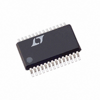
LTC1420CGN Linear Technology, LTC1420CGN Datasheet

LTC1420CGN
Specifications of LTC1420CGN
Available stocks
Related parts for LTC1420CGN
LTC1420CGN Summary of contents
Page 1
... Digital Signal Processing ■ Multiplexed Data Acquisition Systems ■ High Speed Data Acquisition ■ Spectral Analysis ■ Imaging Systems , LTC and LT are registered trademarks of Linear Technology Corporation. All other trademarks are the property of their respective owners. U TYPICAL APPLICATIO 5V 1µF 28 GAIN A ...
Page 2
... REF REF V = 2.048V (SENSE = V ), GAIN = 0V (2×) REF REF External V (SENSE = 5V), GAIN = 5V (1×) REF External V (SENSE = 5V), GAIN = 0V (2×) REF Between Conversions During Conversions –2.048V < (– < 2.048V ORDER PART 28 GAIN NUMBER CLK LTC1420CGN LTC1420IGN 24 GND OGND 80°C/W JA MIN TYP MAX UNITS ● ...
Page 3
ACCURACY otherwise specifications are 25° – 0V. (Note 6) IN SYMBOL PARAMETER S/( Signal-to-Noise Plus Distortion Ratio THD Total Harmonic Distortion SFDR Peak Harmonic or Spurious ...
Page 4
LTC1420 W U POWER REQUIRE E TS range, otherwise specifications are at T (Note 5) SYMBOL PARAMETER V Positive Supply Voltage DD OV Output Supply Voltage DD V Negative Supply Voltage SS I Positive Supply Current DD I Negative Supply ...
Page 5
W U TYPICAL PERFOR A CE CHARACTERISTICS S/(N+D) vs Input Frequency and Amplitude 0dB –6dB IN 65 DUAL SUPPLIES 60 ±2.048V RANGE GAIN = 1× –20dB IN 50 0.1 1 ...
Page 6
LTC1420 W U TYPICAL PERFOR A CE CHARACTERISTICS I vs Clock Frequency 4.096V REF CLOCK FREQUENCY (MHz) CMRR vs Input Frequency ...
Page 7
PIN FUNCTIONS V (Pin 23): Analog 5V Supply. Bypass to GND with a 1µF DD ceramic. GND (Pin 24): Analog Power Ground. V (Pin 25): Negative Supply. Can be – 0V not ...
Page 8
LTC1420 U U APPLICATIONS INFORMATION Conversion Details The LTC1420 is a high performance 12-bit A/D converter that operates up to 10Msps complete solution with an on-chip sample-and-hold, a 12-bit pipelined CMOS ADC, a low drift programmable reference ...
Page 9
U U APPLICATIONS INFORMATION V and V can be driven by an external voltage. With REF REF two additional resistors, V can be set to any voltage REF between 2.048V and 4.5V. An external reference or a DAC can be ...
Page 10
LTC1420 U U APPLICATIONS INFORMATION Table 2. Comparison of Analog Input Configurations SUPPLIES COUPLING V REF DC 4.096V ± 4.096V 5V DC 2.048V 5V DC 4.096V 5V DC 4.096V AC 4.096V ±5V (Transformer 4.096V (Transformer) DC ...
Page 11
U U APPLICATIONS INFORMATION Differential Operation The THD and SFDR performance of the LTC1420 can be improved by using a center tap RF transformer to drive the inputs differentially. Though the signal can no longer be DC coupled, the improvement ...
Page 12
LTC1420 U U APPLICATIONS INFORMATION Digital Outputs and Overflow Bit (OF) Figure 10 shows the ideal input/output characteristics for the LTC1420. The output data is two’s complement binary for all input ranges and for both single and dual supply operation. ...
Page 13
U U APPLICATIONS INFORMATION are present. The SNR performance of an ADC when the performance is limited by jitter is given by: SNR = – 20log (2π ) where f is the frequency of an input ...
Page 14
LTC1420 U U APPLICATIONS INFORMATION 1420fa ...
Page 15
U U APPLICATIONS INFORMATION Figure 15. Top Silkscreen Layer for LTC1420 Demo Board W U Figure 16. Top Layer for LTC1420 Demo Board LTC1420 1420fa 15 ...
Page 16
LTC1420 U U APPLICATIONS INFORMATION Figure 17. Ground Plane Layer for LTC1420 Demo Board Figure 18. Power Plane Layer for LTC1420 Demo Board 1420fa ...
Page 17
U U APPLICATIONS INFORMATION W U Figure 19. Bottom Layer for LTC1420 Demo Board LTC1420 1420fa 17 ...
Page 18
LTC1420 U TYPICAL APPLICATIONS Single Supply, 10Msps, 12-Bit ADC with 3V Logic Outputs ANALOG INPUT (2.5V ±1.024V) 5V 1µF ANALOG INPUT (±2.048V) 5V 1µF 18 LTC1420 30Ω GAIN IN 470pF 2 27 NPO – ...
Page 19
... FLASH SHALL NOT EXCEED 0.010" (0.254mm) PER SIDE Information furnished by Linear Technology Corporation is believed to be accurate and reliable. However, no responsibility is assumed for its use. Linear Technology Corporation makes no representation that the interconnection of its circuits as described herein will not infringe on existing patent rights. ...
Page 20
... DATA 1420 TA05 5 COMMENTS Pin Compatible with the LTC1420 Best Dynamic Performance, SINAD = 72dB at Nyquist 55mW Power Dissipation, 72dB SINAD 0.05% Max Initial Accuracy, 5ppm/°C Max Drift LT/TP 0105 1K • PRINTED IN USA © LINEAR TECHNOLOGY CORPORATION 1999 1420fa ...


