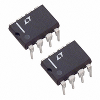
LTC1098CN8 Linear Technology, LTC1098CN8 Datasheet - Page 17

LTC1098CN8
Manufacturer Part Number
LTC1098CN8
Description
IC A/D CONV 8BIT SRL IN/OUT 8DIP
Manufacturer
Linear Technology
Datasheet
1.LTC1098CS8PBF.pdf
(32 pages)
Specifications of LTC1098CN8
Number Of Bits
8
Sampling Rate (per Second)
33k
Data Interface
Serial
Number Of Converters
1
Power Dissipation (max)
780µW
Voltage Supply Source
Single Supply
Operating Temperature
0°C ~ 70°C
Mounting Type
Through Hole
Package / Case
8-DIP (0.300", 7.62mm)
Lead Free Status / RoHS Status
Contains lead / RoHS non-compliant
Available stocks
Company
Part Number
Manufacturer
Quantity
Price
Company:
Part Number:
LTC1098CN8
Manufacturer:
LT
Quantity:
5 510
Company:
Part Number:
LTC1098CN8
Manufacturer:
QTC
Quantity:
5 510
APPLICATIONS INFORMATION
Input Data Word
The LTC1096(L) requires no D
confi gured to have a single differential input. The conver-
sion result, in which output on the D
sequence, followed by LSB sequence providing easy
interface to MSB- or LSB-fi rst serial ports.
The LTC1098(L) clocks data into the D
ing edge of the clock. The input data words are defi ned
as follows:
MSB-FIRST DATA (MSBF = 1)
MSB-FIRST DATA (MSBF = 0)
D
D
D
D
*AFTER COMPLETING THE DATA TRANSFER, IF FURTHER CLOCKS ARE APPLIED WITH CS LOW, THE ADC WILL OUTPUT ZEROS INDEFINITELY.
IN
OUT
IN
OUT
CLK
CLK
t
t
suCS
CS
suCS
CS
HI-Z
HI-Z
START
START
START
t
t
WAKEUP
WAKEUP
SGL/
SGL/
DIFF
DIFF
Figure 2. LTC1098(L) Operating Sequence Example: Differential Inputs (CH
t
t
SMPL
SGL/
SMPL
DIFF
ADDRESS
MUX
ODD/
ODD/
SIGN
SIGN
ODD/
SIGN
IN
MSBF
MSBF
MSB-FIRST/
LSB-FIRST
word. It is permanently
MSBF
10968 AI02
NULL
NULL
BIT
BIT
OUT
IN
(MSB)
(MSB)
B7
B7
line is MSB-fi rst
input on the ris-
B6
B6
t
CYC
B5
B5
t
t
CONV
CONV
DON'T CARE
B4
B4
B3
B3
B2
B2
Start Bit
The fi rst “logical one” clocked into the D
goes low is the start bit. The start bit initiates the data
transfer. The LTC1098(L) will ignore all leading zeros which
precede this logical one. After the start bit is received,
the remaining bits of the input word will be clocked in.
Further inputs on the D
next CS cycle.
t
CYC
B1
B1
B0*
B0
DON'T CARE
B1
POWER
DOWN
Hi-Z
B2
LTC1096/LTC1096L
LTC1098/LTC1098L
B3
B4
IN
pin are then ignored until the
+
B5
, CH
B6
–
)
B7*
IN
POWER
DOWN
Hi-Z
input after CS
10968 F02
17
10968fc


