HI7191IBZ-T Intersil, HI7191IBZ-T Datasheet - Page 14
HI7191IBZ-T
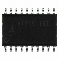
Manufacturer Part Number
HI7191IBZ-T
Description
CONV A/D 24BIT SIGMA/DLTA 20SOIC
Manufacturer
Intersil
Datasheet
1.HI7191IBZ-T.pdf
(25 pages)
Specifications of HI7191IBZ-T
Number Of Bits
24
Data Interface
Serial, SPI™
Number Of Converters
1
Power Dissipation (max)
32.5mW
Voltage Supply Source
Analog and Digital, Dual ±
Operating Temperature
-40°C ~ 85°C
Mounting Type
Surface Mount
Package / Case
20-SOIC (0.300", 7.50mm Width)
Lead Free Status / RoHS Status
Lead free / RoHS Compliant
Other names
HI7191IBZ-TTR
Available stocks
Company
Part Number
Manufacturer
Quantity
Price
Company:

Part Number:
HI7191IBZ-T
Manufacturer:
Intersil
Quantity:
2 000


Scale Calibration Register, and 800000 (h) to the Negative
Full Scale Calibration Register. This sets the offset
correction factor to 0 and both the positive and negative gain
slope factors to 1.
The HI7191 offers several different modes of Self-Calibration
and System Calibration. For calibration to occur, the on-chip
microcontroller must convert the modulator output for three
different input conditions - “zero-scale,” “positive full scale,”
and “negative full scale”. With these readings, the HI7191
can null any offset errors and calculate the gain slope factor
for the transfer function of the converter. It is imperative that
the zero-scale calibration be performed before either of the
gain calibrations. However, the order of the gain calibrations
is not important.
The calibration modes are user selectable in the Control
Register by using the MD bits (MD2-MD0) as shown in
Table 6. DRDY will go low indicating that the calibration is
complete and there is valid data at the output.
Conversion Mode
For Conversion Mode operation the HI7191 converts the
differential voltage between V
switching into this mode it takes 3 conversion periods (3 x
1/f
calibration coefficients are generated when operating in
Conversion Mode as data is calibrated using the existing
calibration coefficients.
Self-Calibration Mode
Please note: Self-calibration is only valid when
operating in a gain of one. In addition, the offset and
gain errors are not reduced as with the full system
calibration.
The Self-Calibration Mode is a three step process that
updates the Offset Calibration Register, the Positive Full
Scale Calibration Register, and the Negative Full Scale
Calibration Register. In this mode an internal offset
calibration is done by disconnecting the external inputs and
shorting the inputs of the PGIA together. After 3 conversion
MD2
N
0
0
0
0
1
1
1
1
) for DRDY to go low and new data to be valid. No
MD1
TABLE 4. HI7191 OPERATIONAL MODES
0
0
1
1
0
0
1
1
MD0
0
1
0
1
0
1
0
1
Conversion
Self Calibration (Gain of 1 only)
System Offset Calibration
System Positive Full Scale Calibration
System Negative Full Scale Calibration
System Offset/Internal Gain Calibration
(Gain of 1 only)
System Gain Calibration
Reserved
14
INHI
OPERATIONAL MODE
and V
INLO
. From
HI7191
periods the Offset Calibration Register is updated with the
value that corrects any internal offset errors.
After the offset calibration is completed the Positive and
Negative Full Scale Calibration Registers are updated. The
inputs V
reference is applied across the modulator inputs. The
HI7191 then takes 3 conversion cycles to sample the data
and update the Positive Full Scale Calibration Register. Next
the polarity of the reference voltage across the modulator
input terminals is reversed and after 3 conversion cycles the
Negative Full Scale Calibration Register is updated. The
values stored in the Positive and Negative Full Scale
Calibration Registers correct for any internal gain errors in
the A/D transfer function. After 3 more conversion cycles the
DRDY line will activate signaling that the calibration is
complete and valid data is present in the Data Output
Register.
System Offset Calibration Mode
The System Offset Calibration Mode is a single step process
that allows the user to lump offset errors of external circuitry
and the internal errors of the HI7191 together and null them
out. This mode will convert the external differential signal
applied to the V
Offset Calibration Register. The user must apply the zero
point or offset voltage to the HI7191 analog inputs and allow
the signal to settle before selecting this mode. After 4
conversion periods the DRDY line will activate signaling that
the calibration is complete and valid data is present in the
Data Output Register.
System Positive Full Scale Calibration Mode
The System Positive Full Scale Calibration Mode is a single
step process that allows the user to lump gain errors of
external circuitry and the internal errors of the HI7191
together and null them out. This mode will convert the
external differential signal applied to the V
stores the converted value in the Positive Full Scale
Calibration Register. The user must apply the +Full Scale
voltage to the HI7191 analog inputs and allow the signal to
settle before selecting this mode. After 4 conversion periods
the DRDY line will activate signaling the calibration is
complete and valid data is present in the Data Output
Register.
System Negative Full Scale Calibration Mode
The System Negative Full Scale Calibration Mode is a
single-step process that allows the user to lump gain errors
of external circuitry and the internal errors of the HI7191
together and null them out. This mode will convert the
external differential signal applied to the V
stores the converted value in the Negative Full Scale
Calibration Register. The user must apply the -Full Scale
voltage to the HI7191 analog inputs and allow the signal to
settle before selecting this mode. After 4 conversion periods
the DRDY line will activate signaling the calibration is
complete and valid data is present in the Data Output
Register.
INHI
and V
IN
inputs and then store that value in the
INLO
are disconnected and the external
IN
IN
inputs and
inputs and
June 1, 2006
FN4138.8
Related parts for HI7191IBZ-T
Image
Part Number
Description
Manufacturer
Datasheet
Request
R

Part Number:
Description:
24-bit, High Precision, Sigma Delta A/d Converter
Manufacturer:
Intersil Corporation
Datasheet:
Part Number:
Description:
Intersil Corporation [CMOS Serial Controller Interface]
Manufacturer:
Intersil Corporation
Datasheet:
Part Number:
Description:
Manufacturer:
Intersil Corporation
Datasheet:
Part Number:
Description:
357-036-542-201 CARDEDGE 36POS DL .156 BLK LOPRO
Manufacturer:
Intersil Corporation
Datasheet:
Part Number:
Description:
1024-Word x 4-Bit LSI Static RAM
Manufacturer:
Intersil Corporation
Datasheet:
Part Number:
Description:
General Purpose NPN Transistor Arrays FN341.4
Manufacturer:
Intersil Corporation
Datasheet:
Part Number:
Description:
CMOS 16-Bit Microprocessor
Manufacturer:
Intersil Corporation
Datasheet:
Part Number:
Description:
Manufacturer:
Intersil Corporation
Datasheet:
Part Number:
Description:
Manufacturer:
Intersil Corporation
Datasheet:
Part Number:
Description:
Manufacturer:
Intersil Corporation
Datasheet:
Part Number:
Description:
Manufacturer:
Intersil Corporation
Datasheet:
Part Number:
Description:
CMOS 6-Bit Latch and Decoder Memory Interfaces
Manufacturer:
Intersil Corporation
Datasheet:
Part Number:
Description:
CA3046General Purpose NPN Transistor Arrays
Manufacturer:
Intersil Corporation
Datasheet:
Part Number:
Description:
Manufacturer:
Intersil Corporation
Datasheet:
Part Number:
Description:
TR909 DLC/FLC SLIC with Low Power Standby
Manufacturer:
Intersil Corporation
Datasheet: