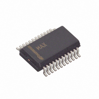
MAX1296BEEG+ Maxim Integrated Products, MAX1296BEEG+ Datasheet - Page 16

MAX1296BEEG+
Manufacturer Part Number
MAX1296BEEG+
Description
IC ADC 12BIT 420KSPS 24-QSOP
Manufacturer
Maxim Integrated Products
Datasheet
1.MAX1296BEEG.pdf
(19 pages)
Specifications of MAX1296BEEG+
Number Of Bits
12
Sampling Rate (per Second)
420k
Data Interface
Parallel
Number Of Converters
1
Power Dissipation (max)
762mW
Voltage Supply Source
Single Supply
Operating Temperature
-40°C ~ 85°C
Mounting Type
Surface Mount
Package / Case
24-QSOP
Number Of Adc Inputs
2
Architecture
SAR
Conversion Rate
420 KSPs
Resolution
12 bit
Voltage Reference
Internal 2.5 V or External
Supply Voltage (max)
5 V
Mounting Style
SMD/SMT
Lead Free Status / RoHS Status
Lead free / RoHS Compliant
tion or conversion can cause additional supplynoise,
which can make it difficult to achieve true 12-bit perfor-
mance.
For best performance, use printed circuit boards. Wire-
wrap configurations are not recommended, since the
layout should ensure proper separation of analog and
digital traces. Do not run analog and digital lines paral-
lel to each other, and don’t lay out digital signal paths
underneath the ADC package. Use separate analog
and digital PC board ground sections with only one star
point (Figure 11) connecting the two ground systems
(analog and digital). For lowest noise operation, ensure
the ground return to the star ground’s power supply is
low impedance and as short as possible. Route digital
signals far away from sensitive analog and reference
inputs.
High-frequency noise in the power supply, V
impair operation of the ADC’s fast comparator. Bypass
V
capacitors, 0.1µF and 4.7µF, located as close to the
MAX1294/MAX1296’s power-supply pin as possible.
Minimize capacitor lead length for best supply-noise
rejection and add an attenuation resistor (5Ω) if the
power supply is extremely noisy.
420ksps, +5V, 6-/2-Channel, 12-Bit ADCs
with +2.5V Reference and Parallel Interface
Figure 10. Timing Diagram for Fastest Conversion
16
DD
D7–D0
STATE
CLK
WR
______________________________________________________________________________________
RD
to the star ground with a network of two parallel
CONTROL
WORD
Layout, Grounding, and Bypassing
1
ACQUISITION
2
D11–
D0
3
SAMPLING INSTANT
4
5
6
7
DD
8
, could
9
CONTROL WORD
CONVERSION
10
Figure 11. Power-Supply and Grounding Connections
11
R* = 5Ω
*OPTIONAL
12
V
+5V
DD
13
4.7µF
0.1µF
14
MAX1294
MAX1296
GND
15
SUPPLIES
16
COM
ACQUISITION
D11–D0
+5V
+5V
CIRCUITRY
DIGITAL
DGND
GND


