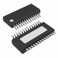
MAX1091BEEI+ Maxim Integrated Products, MAX1091BEEI+ Datasheet - Page 11

MAX1091BEEI+
Manufacturer Part Number
MAX1091BEEI+
Description
IC ADC 10BIT 250KSPS 28-QSOP
Manufacturer
Maxim Integrated Products
Datasheet
1.MAX1093BEEG.pdf
(20 pages)
Specifications of MAX1091BEEI+
Number Of Bits
10
Sampling Rate (per Second)
250k
Data Interface
Parallel
Number Of Converters
1
Power Dissipation (max)
667mW
Voltage Supply Source
Single Supply
Operating Temperature
-40°C ~ 85°C
Mounting Type
Surface Mount
Package / Case
28-QSOP
Number Of Adc Inputs
8
Architecture
SAR
Conversion Rate
250 KSPs
Resolution
10 bit
Input Type
Differential
Interface Type
Parallel
Voltage Reference
Internal 2.5 V or External
Supply Voltage (max)
3 V
Maximum Power Dissipation
762 mW
Maximum Operating Temperature
+ 85 C
Mounting Style
SMD/SMT
Minimum Operating Temperature
- 40 C
Lead Free Status / RoHS Status
Lead free / RoHS Compliant
conversion. The sampling interval occurs at the end of
the acquisition interval. The ACQMOD (acquisition
mode) bit in the input control byte (Table 1) offers two
options for acquiring the signal: an internal and an
external acquisition. The conversion period lasts for 13
clock cycles in either the internal or external clock or
acquisition mode. Writing a new control byte during a
conversion cycle aborts the conversion and starts a
new acquisition interval.
Select internal acquisition by writing the control byte
with the ACQMOD bit cleared (ACQMOD = 0). This
causes the write pulse to initiate an acquisition interval
whose duration is internally timed. Conversion starts
when this acquisition interval ends (three external
cycles or approximately 1µs in internal clock mode)
(Figure 4). Note that, when the internal acquisition is
combined with the internal clock, the aperture jitter can
be as high as 200ps. Internal clock users wishing to
achieve the 50ps jitter specification should always use
external acquisition mode.
Table 1. Control Byte Functional Description
D2, D1, D0
D7, D6
BIT
D5
D4
D3
with +2.5V Reference and Parallel Interface
ACQMOD
PD1, PD0
SGL/DIF
UNI/BIP
A2, A1, A0
NAME
______________________________________________________________________________________
250ksps, +3V, 8-/4-Channel, 10-Bit ADCs
PD1 and PD0 select the various clock and power-down modes.
ACQMOD = 0: Internal Acquisition Mode
ACQMOD = 1: External Acquisition Mode
SGL/DIF = 0: Pseudo-Differential Analog Input Mode
SGL/DIF = 1: Single-Ended Analog Input Mode
In single-ended mode, input signals are referred to COM. In pseudo-differential mode, the voltage
difference between two channels is measured (see Tables 2 and 3).
UNI/BIP = 0: Bipolar Mode
UNI/BIP = 1: Unipolar Mode
In unipolar mode, an analog input signal from 0 to V
nal can range from -V
Address bits A2, A1, A0 select which of the 8/4 (MAX1091/MAX1093) channels are to be converted
(see Tables 3 and 4).
0
0
1
1
Internal Acquisition
0
1
0
1
Full Power-Down Mode. Clock mode is unaffected.
Standby Power-Down Mode. Clock mode is unaffected.
Normal Operation Mode. Internal clock mode selected.
Normal Operation Mode. External clock mode selected.
REF
/2 to +V
REF
/2.
Use external acquisition mode for precise control of the
sampling aperture and/or dependent control of acquisi-
tion and conversion times. The user controls acquisition
and start-of-conversion with two separate write pulses.
The first pulse, written with ACQMOD = 1, starts an
acquisition interval of indeterminate length. The second
write pulse, written with ACQMOD = 0, terminates
acquisition and starts conversion on WR’s rising edge
(Figure 5).
The address bits for the input multiplexer must have the
same values on the first and second write pulse.
Power-down mode bits (PD0, PD1) can assume new
values on the second write pulse (see the Power-Down
Modes section). Changing other bits in the control byte
corrupts the conversion.
A standard interrupt signal INT is provided to allow the
MAX1091/MAX1093 to flag the µP when the conversion
has ended and a valid result is available. INT goes low
when the conversion is complete and the output data is
ready (Figures 4 and 5). It returns high on the first read
cycle or if a new control byte is written.
FUNCTION
REF
can be converted; in bipolar mode, the sig-
Reading a Conversion
External Acquisition
11


