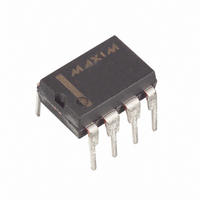
MAX1241BCPA+ Maxim Integrated Products, MAX1241BCPA+ Datasheet - Page 7

MAX1241BCPA+
Manufacturer Part Number
MAX1241BCPA+
Description
IC ADC SERIAL 12BIT 2.7V 8-DIP
Manufacturer
Maxim Integrated Products
Datasheet
1.MAX1241BCSA.pdf
(15 pages)
Specifications of MAX1241BCPA+
Number Of Bits
12
Sampling Rate (per Second)
73k
Data Interface
MICROWIRE™, QSPI™, Serial, SPI™
Number Of Converters
1
Power Dissipation (max)
727mW
Voltage Supply Source
Single Supply
Operating Temperature
0°C ~ 70°C
Mounting Type
Through Hole
Package / Case
8-DIP (0.300", 7.62mm)
Number Of Adc Inputs
1
Architecture
SAR
Conversion Rate
73 KSPs
Resolution
12 bit
Input Type
Voltage
Voltage Reference
External
Supply Voltage (max)
5.25 V
Supply Voltage (min)
2.7 V
Maximum Power Dissipation
727 mW
Maximum Operating Temperature
+ 70 C
Mounting Style
Through Hole
Minimum Operating Temperature
0 C
Lead Free Status / RoHS Status
Lead free / RoHS Compliant
(V
_______________________________________________________________________Pin Description
____________________________Typical Operating Characteristics (continued)
DD
PIN
= 3.0V, REF = 2.5V, f
1
2
3
4
5
6
7
8
-0.2
-0.4
-0.6
0.6
0.4
0.2
0
0
NAME
SHDN
DOUT
SCLK
GND
REF
V
AIN
CS
DD
INTEGRAL NONLINEARITY
_______________________________________________________________________________________
1024
SCLK
vs. CODE
Positive Supply Voltage: 2.7V to 3.6V, (MAX1240); 2.7V to 5.25V (MAX1241)
Sampling Analog Input, 0V to V
Three-Level Shutdown Input. Pulling SHDN low shuts the MAX1240/MAX1241 down to 15µA (max)
supply current. Both the MAX1240 and MAX1241 are fully operational with either SHDN high or
unconnected. For the MAX1240, pulling SHDN high enables the internal reference, and letting SHDN
open disables the internal reference and allows for the use of an external reference.
Reference Voltage for Analog-to-Digital Conversion. Internal 2.5V reference output for MAX1240;
bypass with 4.7µF capacitor. External reference voltage input for MAX1241, or for MAX1240 with the
internal reference disabled. Bypass REF with a minimum of 0.1µF when using an external reference.
Analog and Digital Ground
Serial Data Output. Data changes state at SCLK’s falling edge. DOUT is high impedance when CS is
high.
Active-Low Chip Select initiates conversions on the falling edge. When CS is high, DOUT is high
impedance.
Serial Clock Input. SCLK clocks data out at rates up to 2.1MHz.
CODE
2048
= 2.1MHz, C
3072
L
4096
= 20pF, T
12-Bit Serial ADCs in 8-Pin SO
A
= +25°C, unless otherwise noted.)
REF
range
-100
-120
-140
FUNCTION
-20
-40
-60
-80
20
0
0
+2.7V, Low-Power,
FREQUENCY (kHz)
FFT PLOT
18.75
f
f
AIN
SAMPLE
= 10kHz, 2.5V
= 73ksps
P-P
37.50
7


