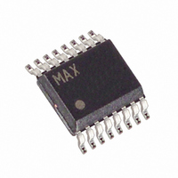
MAX11615EEE+ Maxim Integrated Products, MAX11615EEE+ Datasheet - Page 4

MAX11615EEE+
Manufacturer Part Number
MAX11615EEE+
Description
IC ADC SERIAL 12BIT 8CH 16-QSOP
Manufacturer
Maxim Integrated Products
Datasheet
1.MAX11612EUA.pdf
(22 pages)
Specifications of MAX11615EEE+
Number Of Bits
12
Sampling Rate (per Second)
94.4k
Data Interface
I²C, Serial
Number Of Converters
1
Power Dissipation (max)
666.7mW
Voltage Supply Source
Single Supply
Operating Temperature
-40°C ~ 85°C
Mounting Type
Surface Mount
Package / Case
16-SSOP (0.150", 3.90mm Width)
Resolution
12 bit
Interface Type
I2C
Snr
70 dB
Voltage Reference
2.048 V
Supply Voltage (max)
3.6 V
Supply Voltage (min)
2.7 V
Maximum Power Dissipation
666.7 mW
Maximum Operating Temperature
+ 85 C
Mounting Style
SMD/SMT
Input Voltage
3.3 V
Minimum Operating Temperature
- 40 C
Lead Free Status / RoHS Status
Lead free / RoHS Compliant
Low-Power, 4-/8-/12-Channel, I
12-Bit ADCs in Ultra-Small Packages
ELECTRICAL CHARACTERISTICS (continued)
(V
(MAX11613/MAX11615/MAX11617), V
otherwise noted. Typical values are at T
TIMING CHARACTERISTICS (Figure 1)
(V
(MAX11613/MAX11615/MAX11617), V
otherwise noted. Typical values are at T
4
TIMING CHARACTERISTICS FOR FAST MODE
Serial-Clock Frequency
Bus Free Time Between a STOP (P)
and a START (S) Condition
Hold Time for START (S) Condition
Low Period of the SCL Clock
High Period of the SCL Clock
Setup Time for a Repeated START
Condition (Sr)
Data Hold Time (Note 11)
Data Setup Time
Rise Time of Both SDA and SCL
Signals, Receiving
Fall Time of SDA Transmitting
Setup Time for STOP (P) Condition
Capacitive Load for Each Bus Line
Pulse Width of Spike Suppressed
POWER REQUIREMENTS
Supply Voltage
Supply Current
Power-Supply Rejection Ratio
DD
DD
_______________________________________________________________________________________
= 2.7V to 3.6V (MAX11613/MAX11615/MAX11617), V
= 2.7V to 3.6V (MAX11613/MAX11615/MAX11617), V
PARAMETER
PARAMETER
SYMBOL
SYMBOL
t
t
t
t
t
REF
REF
HD, DAT
HD, STA
SU, DAT
SU, STO
SU, STA
PSRR
t
t
A
V
A
t
f
HIGH
I
LOW
BUF
SCL
C
t
DD
t
DD
t
SP
R
= +25°C, see Tables 1–5 for programming notation.) (Note 1)
= +25°C, see Tables 1–5 for programming notation.) (Note 1)
F
B
= 4.096V (MAX11612/MAX11614/MAX11616), f
= 4.096V (MAX11612/MAX11614/MAX11616), f
MAX11613/MAX11615/MAX11617
MAX11612/MAX11614/MAX11616
f
external clock
f
internal clock
f
internal clock
f
internal clock
Shutdown (internal REF off)
Full-scale input (Note 10)
Measured from 0.3V
Measured from 0.3V
SAMPLE
SAMPLE
SAMPLE
SAMPLE
= 94.4ksps
= 40ksps
= 10ksps
=1ksps
DD
DD
= 4.5V to 5.5V (MAX11612/MAX11614/MAX11616), V
= 4.5V to 5.5V (MAX11612/MAX11614/MAX11616), V
CONDITIONS
CONDITIONS
DD
DD
- 0.7V
- 0.7V
Internal reference
External reference
Internal reference
External reference
Internal reference
External reference
Internal reference
External reference
DD
DD
(Note 12)
2
C,
SCL
SCL
= 1.7MHz, T
= 1.7MHz, T
20 + 0.1C
20 + 0.1C
MIN
MIN
100
1.3
0.6
1.3
0.6
0.6
0.6
2.7
4.5
0
B
B
A
A
TYP
TYP
±0.5
900
670
530
230
380
330
0.5
60
6
= T
= T
MIN
MIN
1150
MAX
MAX
±2.0
400
900
300
300
400
to T
900
to T
3.6
5.5
50
10
REF
REF
MAX
MAX
= 2.048V
= 2.048V
, unless
, unless
UNITS
UNITS
LSB/V
kHz
pF
µA
µs
µs
µs
µs
µs
ns
ns
ns
ns
µs
ns
V


