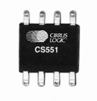
CS5513-BSZ Cirrus Logic Inc, CS5513-BSZ Datasheet - Page 10

CS5513-BSZ
Manufacturer Part Number
CS5513-BSZ
Description
IC ADC 20BIT INTERNAL OSC 8SOIC
Manufacturer
Cirrus Logic Inc
Datasheet
1.CS5513-BSZ.pdf
(26 pages)
Specifications of CS5513-BSZ
Data Interface
Serial
Number Of Bits
20
Sampling Rate (per Second)
326
Number Of Converters
1
Power Dissipation (max)
2.7mW
Voltage Supply Source
Dual ±
Operating Temperature
-40°C ~ 85°C
Mounting Type
Surface Mount
Package / Case
8-SOIC (0.200", 5.30mm Width)
Resolution (bits)
20bit
Sampling Rate
100SPS
Input Channel Type
Differential
Supply Voltage Range - Analog
4.75V To 5.25V
Supply Current
385µA
Digital Ic Case Style
SOIC
Lead Free Status / RoHS Status
Lead free / RoHS Compliant
Other names
598-1707
Available stocks
Company
Part Number
Manufacturer
Quantity
Price
Part Number:
CS5513-BSZ
Manufacturer:
CIRRUS
Quantity:
20 000
2. GENERAL DESCRIPTION
The CS5510/11/12/13 are low-cost, easy-to-use,
ΔΣ analog-to-digital converters (ADCs) which use
charge balance techniques to achieve 16-bit
(CS5510/11) and 20-bit (CS5512/13) perfor-
mance. The ADCs are available in a space-effi-
cient, 8-pin, SOIC package and are optimized for
measuring signals in weigh scale, process control,
and other industrial applications.
To accommodate these applications, the ADCs in-
clude a fourth-order ΔΣ modulator and a digital fil-
ter. When configured with an external master clock
of 32.768 kHz, the filter in the CS5510/12 provides
better than 80 dB of simultaneous 50 and 60 Hz
line rejection, and outputs conversion words at
53.5 Sps. The CS5511/13 include an on-chip oscil-
lator which eliminates the need for an external
clock source.
The CS5510/11/12/13 ADCs are designed to oper-
ate from a single +5 V supply or a variety dual-sup-
ply configurations and are optimized to digitize
bipolar signals in industrial applications.
To achieve low cost, the CS5510/11/12/13 family
of converters have no on-chip calibration features.
The CS5510/11/12/13 offer very low offset drift,
low gain drift, and excellent linearity.
2.1
The CS5510/11/12/13 provides a differential input
span of approximately ±(0.80 ± 0.08) times the dif-
10
Analog Input
V
i = f V
o s
n
≤ 2 5 mV
AIN
Figure 3. Input models for AIN+ and AIN- pins.
os
C
f = 32.768 kHz
ferential voltage reference (VREF - V-). This trans-
lates to typically ±4.0 V fully differential when the
reference voltage between VREF and V- is 5 V,
and typically ±2.0 V fully differential at 2.5 V.
Note:
2.1.1
Figure 3 illustrates the input model for the AIN
pins. The model includes a coarse/fine charge
buffer which reduces the dynamic current de-
mands from the signal source. The buffer is de-
signed to accommodate rail-to-rail (common-mode
plus signal) input voltages. Typical CVF (sampling)
current is about 10 nA. Application Note 30,
“Switched-capacitor A/D Input Structures”, details
various input architectures.
2.2
The voltage between the VREF and V- pins of the
converter determines the voltage reference for the
converter. This voltage can be as low as 250 mV,
or as great as (V+) - (V-). The VREF pin can be
connected directly to the V+ pin. This will establish
a voltage reference equal to (V+) - (V-) for the con-
verter. The effective resolution of the part (noise-
free bits for a single sample with no averaging) will
vary with VREF. Figure 4 shows how the VREF
voltage affects the noise-free resolution of the
φ Coarse
1
φ Fine
1
C = 12 p F
Voltage Reference Input
When a smaller reference voltage is used,
the resulting code widths are smaller. Since
the output codes exhibit more changing
codes for a fixed amount of noise, the
converter appears noisier.
Analog Input Model
CS5510/11/12/13
DS337F4


