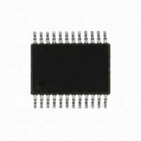
CS5550-ISZ Cirrus Logic Inc, CS5550-ISZ Datasheet - Page 10

CS5550-ISZ
Manufacturer Part Number
CS5550-ISZ
Description
IC ADC 2CH LOW-COST 24SSOP
Manufacturer
Cirrus Logic Inc
Datasheet
1.CS5550-ISZ.pdf
(24 pages)
Specifications of CS5550-ISZ
Number Of Converters
2
Package / Case
24-SSOP
Number Of Bits
2
Sampling Rate (per Second)
4k
Data Interface
Serial
Power Dissipation (max)
30mW
Voltage Supply Source
Analog and Digital
Operating Temperature
-40°C ~ 85°C
Mounting Type
Surface Mount
Number Of Adc Inputs
2
Architecture
Delta-Sigma
Conversion Rate
4 KSPs
Resolution
24 bit
Input Type
Voltage
Interface Type
Serial (3-Wire)
Voltage Reference
2.5 V
Supply Voltage (max)
5 V
Supply Voltage (min)
3.3 V
Maximum Operating Temperature
+ 85 C
Mounting Style
SMD/SMT
Input Voltage
3.3 V to 5 V
Minimum Operating Temperature
- 40 C
Lead Free Status / RoHS Status
Lead free / RoHS Compliant
Lead Free Status / RoHS Status
Lead free / RoHS Compliant, Lead free / RoHS Compliant
Other names
598-1119-5
Available stocks
Company
Part Number
Manufacturer
Quantity
Price
Part Number:
CS5550-ISZ
Manufacturer:
CIRRUS
Quantity:
20 000
2.1 Theory of Operation
The analog signals at the analog inputs are subject
to the gains of the input PGAs. These signals are
then sampled by the delta-sigma modulators at a
rate of (MCLK/K) / 8.
2.1.1 High-Rate Digital Low-Pass Filters
The data is then low-pass filtered, to remove
high-frequency noise from the modulator output.
The high rate filters on both channels are imple-
mented as fixed Sinc
2.1.2 Digital Compensation Filters
The data from both channels is then passed
through two 4th-order IIR “compensation” filters,
whose purpose is to correct (compensate) for the
magnitude roll-off of the low-pass filtering opera-
tion. These filters “re-flatten” the magnitude re-
sponse of the AIN1 and AIN2 channels over the
relevant frequency range, by correcting for the
magnitude roll-off effects that are induced by the
Sinc
2.1.3 Gain and Offset Adjustment
After the filtering, the digital codes are subjected to
value adjustments, based on the values in the DC
Offset Registers (additive) and the Gain Registers
(multiplicative). These registers are used for cali-
bration of the device (see Section 3.4, Calibration).
After offset and gain, the data is available to the
user by reading the appropriate registers.
2.2 Performing Measurements
The CS5550 performs measurements at an output
word rate (sampling rate) of (MCLK/K) / 1024.
From these instantaneous samples, FILT
FILT
stantaneous samples that were acquired. All of the
measurements/results are available as a percent-
age of full scale. The signed output format is a
two’s complement format, and the output data
words represent a normalized value between -1
and +1. The unsigned data in the CS5550 output
registers represent normalized values between 0
and 1. A register value of 1 represents the maxi-
mum possible value. Note that a value of 1.0 is
never actually obtained, the true maximum register
value is [(2^23 - 1) / (2^23)] = 0.999999880791.
10
3
2
low-pass filter stages.
are computed, using the most recent N in-
3
filters.
1
and
After each A/D conversion, the CRDY bit will be as-
serted in the Status Register, and the INT pin will
also become active if the CRDY bit is unmasked (in
the Mask Register). The assertion of the CRDY bit
indicates that new instantaneous samples have
been collected.
The unsigned FILT
dated every N conversions (which is known as 1
“computation cycle”) where N is the value in the
Cycle Count Register. At the end of each computa-
tion cycle, the DRDY bit in the Mask Register will
be set, and the INT pin will become active if the
DRDY bit is unmasked.
DRDY is set only after each computation cycle has
completed, whereas the CRDY bit is asserted after
each individual A/D conversion. When these bits
are asserted, they must be cleared before they can
be asserted again. If the Cycle Count Register val-
ue (N) is set to 1, all output calculations are instan-
taneous,
instantaneous calculations are finished, just like
the CRDY bit. For the FILT results to be valid, the
Cycle-Count Register must be set to a value great-
er than 10.
A computation cycle is derived from the master
clock and its frequency is (MCLK/K)/(1024*N). Un-
der default conditions with a 4.096 MHz clock at
XIN, instantaneous A/D conversions are per-
formed at a 4000 Hz rate, whereas FILT calcula-
tions are performed at a 1 Hz rate.
2.3 CS5550 Linearity Performance
Table 2 lists the range of input levels (as a percent-
age of full-scale registration in the FILT Registers)
over which the output linearity of the FILT Register
measurements are guaranteed to be within
Range (% of FS)
Table 2. Available range of ±0.1% output
linearity, with default settings in the
Linearity
gain/offset registers.
and
DRDY
1
0.2% - 100%
and FILT
0.1% of
reading
FILT
1
will
2
1% - 100%
0.1% of
calculations are up-
reading
FILT
indicate
2
CS5550
DS630F1
±
0.1%.
when


