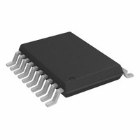
AD7908BRUZ Analog Devices Inc, AD7908BRUZ Datasheet - Page 17

AD7908BRUZ
Manufacturer Part Number
AD7908BRUZ
Description
IC ADC 8BIT 8CH 1MSPS 20-TSSOP
Manufacturer
Analog Devices Inc
Specifications of AD7908BRUZ
Data Interface
DSP, MICROWIRE™, QSPI™, Serial, SPI™
Number Of Bits
8
Sampling Rate (per Second)
1M
Number Of Converters
1
Power Dissipation (max)
13.5mW
Voltage Supply Source
Single Supply
Operating Temperature
-40°C ~ 85°C
Mounting Type
Surface Mount
Package / Case
20-TSSOP (0.173", 4.40mm Width)
Resolution (bits)
8bit
Sampling Rate
1MSPS
Input Channel Type
Single Ended
Supply Voltage Range - Analog
2.7V To 5.25V
Supply Current
2.7mA
Digital Ic Case Style
TSSOP
Lead Free Status / RoHS Status
Lead free / RoHS Compliant
For Use With
EVAL-AD79X8CBZ - BOARD EVALUATION FOR AD79X8
Lead Free Status / RoHS Status
Lead free / RoHS Compliant, Lead free / RoHS Compliant
Available stocks
Company
Part Number
Manufacturer
Quantity
Price
Company:
Part Number:
AD7908BRUZ
Manufacturer:
ADI
Quantity:
1 000
Part Number:
AD7908BRUZ
Manufacturer:
ADI/亚德诺
Quantity:
20 000
Company:
Part Number:
AD7908BRUZ-REEL
Manufacturer:
ADI
Quantity:
1 000
SHADOW REGISTER
MSB
V
The SHADOW register on the AD7908/AD7918/AD7928 is a
16-bit, write-only register. Data is loaded from the DIN pin of
the AD7908/AD7918/AD7928 on the falling edge of SCLK. The
data is transferred on the DIN line at the same time that a
conversion result is read from the part. This requires 16 serial
clock falling edges for the data transfer. The information is
clocked into the SHADOW register, provided that the SEQ and
SHADOW bits were set to 0,1, respectively, in the previous
write to the control register. MSB denotes the first bit in the
data stream. Each bit represents an analog input from Channel 0
to Channel 7. Through programming the SHADOW register,
two sequences of channels can be selected, through which the
AD7908/AD7918/AD7928 cycle with each consecutive
conversion after the write to the SHADOW register.
Sequence One is performed first and then Sequence Two. If the
user does not wish to perform a second sequence option, then
all 0s must be written to the last 8 LSBs of the SHADOW
register. To select a sequence of channels, the associated channel
bit must be set for each analog input. The AD7908/AD7918/
AD7928 continuously cycle through the selected channels in
ascending order beginning with the lowest channel, until a
write operation occurs (that is, the WRITE bit is set to 1) with
the SEQ and SHADOW bits configured in any way except 1, 0,
(see Table 10). The bit functions are outlined in the SHADOW
register bit map.
Figure 11 reflects the traditional operation of a multichannel
ADC, where each serial transfer selects the next channel for
conversion. In this mode of operation the sequencer function is
not used.
Figure 12 shows how to program the AD7908/AD7918/AD7928
to continuously convert on a particular sequence of channels.
To exit this mode of operation and revert back to the traditional
mode of operation of a multichannel ADC (as outlined in
Figure 11), ensure that the WRITE bit = 1 and the SEQ =
SHADOW = 0 on the next serial transfer. Figure 13 shows how
a sequence of consecutive channels can be converted on without
having to program the SHADOW register or write to the part
on each serial transfer. Again, to exit this mode of operation and
revert back to the traditional mode of operation of a multichannel
ADC (as outlined in Figure 11), ensure the WRITE bit = 1 and
the SEQ = SHADOW = 0 on the next serial transfer.
IN
0
V
IN
1
V
IN
2
Sequence One
V
IN
3
V
IN
4
V
IN
5
V
IN
6
Rev. B | Page 17 of 28
V
IN
7
V
IN
0
CS
CS
CS
CS
CS
V
WRITE BIT = 0
IN
1
DIN: WRITE TO CONTROL REGISTER,
WRITE BIT = 1, SELECT CODING, RANGE,
AND POWER MODE.
SELECT A2 TO A0 FOR CONVERSION.
SEQ = SHADOW = 0
DOUT: CONVERSION RESULT FROM
PREVIOUSLY SELECTED
CHANNEL A2 TO A0.
DIN: WRITE TO CONTROL REGISTER,
WRITE BIT = 1, SELECT CODING, RANGE,
AND POWER MODE.
SELECT A2 TO A0 FOR CONVERSION.
SEQ = SHADOW = 0
Figure 11. SEQ Bit = 0, SHADOW Bit = 0 Flowchart
Figure 12. SEQ Bit = 0, SHADOW Bit = 1 Flowchart
CONTINUOUSLY
CONVERTS ON
THE SELECTED
SEQUENCE OF
CHANNELS
V
WRITE BIT = 0
DIN: WRITE TO CONTROL REGISTER,
WRITE BIT = 1, SELECT CODING, RANGE,
AND POWER MODE.
SELECT CHANNEL A2 TO A0
FOR CONVERSION.
SEQ = 0 SHADOW = 1
DOUT: CONVERSION RESULT FROM
PREVIOUSLY SELECTED CHANNEL A2
TO A0.
DIN: WRITE TO SHADOW REGISTER,
SELECTING WHICH CHANNELS TO
CONVERT ON; CHANNELS SELECTED
NEED NOT BE CONSECUTIVE
CHANNELS
IN
WRITE BIT = 0
2
DUMMY CONVERSION
DIN = ALL 1s
POWER-ON
Sequence Two
DUMMY CONVERSION
V
IN
AD7908/AD7918/AD7928
3
DIN = ALL 1s
POWER-ON
SEQ = 1, SHADOW = 0
CONTINUOUSLY
CONVERTS ON THE
SELECTED SEQUENCE
OF CHANNELS BUT WILL
ALLOW RANGE, CODING,
AND SO ON, TO CHANGE
IN THE CONTROL
REGISTER WITHOUT
INTERRUPTING THE
SEQUENCE, PROVIDED
SEQ = 1 SHADOW = 0
V
IN
WRITE BIT = 1
SEQ = 1, SHADOW = 0
4
WRITE BIT = 1
V
IN
5
WRITE BIT = 1,
SEQ = SHADOW = 0
V
IN
6
V
IN
LSB
7


