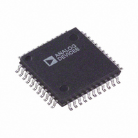
AD73322AST Analog Devices Inc, AD73322AST Datasheet - Page 19

AD73322AST
Manufacturer Part Number
AD73322AST
Description
IC ANALOG FRONT END DUAL 44-LQFP
Manufacturer
Analog Devices Inc
Datasheet
1.AD73322LARUZ-REEL.pdf
(43 pages)
Specifications of AD73322AST
Rohs Status
RoHS non-compliant
Number Of Bits
16
Number Of Channels
4
Power (watts)
73mW
Voltage - Supply, Analog
2.7 V ~ 5.5 V
Voltage - Supply, Digital
2.7 V ~ 5.5 V
Package / Case
44-LQFP
Available stocks
Company
Part Number
Manufacturer
Quantity
Price
Company:
Part Number:
AD73322AST
Manufacturer:
ADI
Quantity:
201
Part Number:
AD73322AST
Manufacturer:
ADI/亚德诺
Quantity:
20 000
The SPORT can work at four different serial clock (SCLK)
rates: chosen from DMCLK, DMCLK/2, DMCLK/4 or
DMCLK/8, where DMCLK is the internal or device master
clock resulting from the external or pin master clock being
divided by the master clock divider.
SPORT Register Maps
There are two register banks for each codec in the AD73322:
the control register bank and the data register bank. The con-
trol register bank consists of eight read/write registers, each
eight bits wide. Table XII shows the control register map for
the AD73322. The first two control registers, CRA and CRB,
are reserved for controlling the SPORT. They hold settings for
parameters such as serial clock rate, internal master clock rate,
sample rate and device count. As both codecs are internally
cascaded, registers CRA and CRB on each codec must be pro-
grammed with the same setting to ensure correct operation (this
is shown in the programming examples). The other five regis-
ters; CRC through CRH are used to hold control settings for
the ADC, DAC, Reference, Power Control and Gain Tap
sections of the device. It is not necessary that the contents of
CRC through CRH on each codec be similar. Control regis-
ters are written to on the negative edge of SCLK. The data
register bank consists of two 16-bit registers that are the DAC
and ADC registers.
Master Clock Divider
The AD73322 features a programmable master clock divider
that allows the user to reduce an externally available master
clock, at pin MCLK, by one of the ratios 1, 2, 3, 4 or 5 to pro-
duce an internal master clock signal (DMCLK) that is used to
calculate the sampling and serial clock rates. The master clock
divider is programmable by setting CRB:4-6. Table VIII shows
the division ratio corresponding to the various bit settings. The
default divider ratio is divide-by-one.
MCD2
0
0
0
0
1
1
1
1
Serial Clock Rate Divider
The AD73322 features a programmable serial clock divider that
allows users to match the serial clock (SCLK) rate of the data to
that of the DSP engine or host processor. The maximum SCLK
rate available is DMCLK and the other available rates are:
DMCLK/2, DMCLK/4 and DMCLK/8. The slowest rate
(DMCLK/8) is the default SCLK rate. The serial clock divider
is programmable by setting bits CRB:2–3. Table IX shows the
serial clock rate corresponding to the various bit settings.
REV. B
Table VIII. DMCLK (Internal) Rate Divider Settings
MCD1
0
0
1
1
0
0
1
1
MCD0
0
1
0
1
0
1
0
1
DMCLK Rate
MCLK
MCLK/2
MCLK/3
MCLK/4
MCLK/5
MCLK
MCLK
MCLK
–19–
Sample Rate Divider
The AD73322 features a programmable sample rate divider that
allows users flexibility in matching the codec’s ADC and DAC
sample rates (decimation/interpolation rates)to the needs of the
DSP software. The maximum sample rate available is DMCLK/
256, which offers the lowest conversion group delay, while the
other available rates are: DMCLK/512, DMCLK/1024 and
DMCLK/2048. The slowest rate (DMCLK/2048) is the default
sample rate. The sample rate divider is programmable by set-
ting bits CRB:0-1. Table X shows the sample rate correspond-
ing to the various bit settings.
DAC Advance Register
The loading of the DAC is internally synchronized with the
unloading of the ADC data in each sampling interval. The de-
fault DAC load event happens one SCLK cycle before the
SDOFS flag is raised by the ADC data being ready. However,
this DAC load position can be advanced before this time by
modifying the contents of the DAC advance field in Control
Register E (CRE:0–4). The field is five bits wide, allowing 31
increments of weight 1/(F
F
the Sample Rate divider; see Tables VIII and X. In certain cir-
cumstances this DAC update adjustment can reduce the group
delay when the ADC and DAC are used to process data in
series. Appendix C details how the DAC advance feature can be
used.
NOTE: The DAC advance register should not be changed while
the DAC section is powered up.
DA4
0
0
0
—
1
1
S
is dependent on the setting of both the MCLK divider and
DA3
0
0
0
—
1
1
Table X. Sample Rate Divider Settings
SCD1
0
0
1
1
DIR1
0
0
1
1
Table IX. SCLK Rate Divider Settings
Table XI. DAC Timing Control
DA2
0
0
0
—
1
1
DIR0
0
1
0
1
SCD0
0
1
0
1
S
DA1
0
0
1
—
1
1
32); see Table XI. The sample rate
SCLK Rate
DMCLK/2048
DMCLK/1024
DMCLK/512
DMCLK/256
DA0
0
1
0
—
0
1
SCLK Rate
DMCLK/8
DMCLK/4
DMCLK/2
DMCLK
AD73322
Time Advance
0 s
1/(F
2/(F
—
30/(F
31/(F
S
S
S
S
32) s
32) s
32) s
32) s


