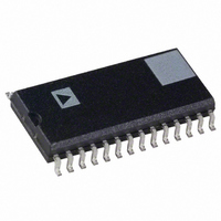
AD73322AR Analog Devices Inc, AD73322AR Datasheet - Page 17

AD73322AR
Manufacturer Part Number
AD73322AR
Description
IC ANALOG FRONT END DUAL 28-SOIC
Manufacturer
Analog Devices Inc
Datasheet
1.AD73322LARUZ-REEL.pdf
(43 pages)
Specifications of AD73322AR
Rohs Status
RoHS non-compliant
Number Of Bits
16
Number Of Channels
4
Power (watts)
73mW
Voltage - Supply, Analog
2.7 V ~ 5.5 V
Voltage - Supply, Digital
2.7 V ~ 5.5 V
Package / Case
28-SOIC (7.5mm Width)
Single Supply Voltage (min)
2.7V
Single Supply Voltage (max)
3.3V
Package Type
SOIC W
Lead Free Status / RoHS Status
Not Compliant
Available stocks
Company
Part Number
Manufacturer
Quantity
Price
Part Number:
AD73322AR-REEL
Manufacturer:
ADI/亚德诺
Quantity:
20 000
Company:
Part Number:
AD73322ARZ
Manufacturer:
2002+
Quantity:
6 219
Part Number:
AD73322ARZ
Manufacturer:
ADI/亚德诺
Quantity:
20 000
REV. B
Differential Output Amplifiers
The decoder has a differential analog output pair (VOUTP and
VOUTN). The output channel can be muted by setting the
MUTE bit (CRD:7) in Control Register D. The output signal is
dc-biased to the codec’s on-chip voltage reference.
Voltage Reference
The AD73322 reference, REFCAP, is a bandgap reference that
provides a low noise, temperature-compensated reference to the
DAC and ADC. A buffered version of the reference is also made
available on the REFOUT pin and can be used to bias other
external analog circuitry. The reference has a default nominal
value of 1.2 V, but can be set to a nominal value of 2.4 V by
setting the 5VEN bit (CRC:7) of CRC. The 5 V mode is gener-
ally only usable when AV
REFCAP
REFOUT
VOUTP1
VOUTN1
VFBN1
VFBP1
VINN1
VINP1
INVERTING
OP AMPS
RESET
SDIFS
SDI
SE
REGISTER
CONTROL
V
Figure 13. Analog Input/Output Section
REF
1A
8
EXTERNAL
DIVIDER
MCLK
LOOP-BACK
MCLK
3
ANALOG
SELECT
REGISTER
CONTROL
+6/–15dB
1B
DD
8
DMCLK INTERNAL
CONTROL
REGISTER
CONTROL
REGISTER
PGA
16
= 5 V.
SERIAL REGISTER 1
1G
1H
REFERENCE
SERIAL PORT 1
REGISTER
CONTROL
(SPORT 1)
GAIN
CONTINUOUS
8
1
LOW-PASS
1C
FILTER
TIME
REGISTER
CONTROL
INVERT
1F
8
8
REGISTER
CONTROL
1D
Figure 14. SPORT Block Diagram
ANALOG GAIN
V
AD73322
REF
8
DIVIDER
SCLK
TAP
2
0/38dB
SINGLE-
ENABLE
ENDED
PGA
REGISTER
CONTROL
1E
SCLK
SDOFS1
SDO1
–17–
The reference output (REFOUT) can be enabled for biasing
external circuitry by setting the RU bit (CRC:6) of CRC.
Analog and Digital Gain Taps
The AD73322 features analog and digital feedback paths be-
tween input and output. The amount of feedback is determined
by the gain setting which is programmed in the control registers.
This feature can typically be used for balancing the effective
impedance between input and output when used in Subscriber
Line Interface Circuit (SLIC) interfacing.
Analog Gain Tap
The analog gain tap is configured as a programmable differential
amplifier whose input is taken from the ADC’s input signal path.
The output of the analog gain tap is summed with the output of
the DAC. The gain is programmable using Control Register F
(CRF:0-4) to achieve a gain of –1 to +1 in 32 steps with muting
being achieved through a separate control setting (Control Regis-
ter F Bit 7). The gain increment per step is 0.0625. The AGT is
enabled by powering-up the AGT control bit in the power con-
trol register (CRC:1). When this bit is set (=1) CRF becomes an
AGT control register with CRF:0-4 holding the AGT coeffi-
cient, CRF:5 becomes an AGT enable and CRF:7 becomes an
AGT mute control bit. Control bit CRF:5 connects/disconnects
the AGT output to the summer block at the output of the DAC
section while control bit CRF:7 overrides the gain tap setting
with a mute, (zero gain) setting. Table VI shows the gain versus
digital setting for the AGT.
SDIFS2
RESET
REGISTER
CONTROL
SDI2
SE
2A
8
EXTERNAL
DIVIDER
MCLK
MCLK
3
REGISTER
CONTROL
2B
8
DMCLK INTERNAL
CONTROL
REGISTER
CONTROL
REGISTER
16
SERIAL REGISTER 2
2G
2H
SERIAL PORT 2
REGISTER
CONTROL
(SPORT 2)
8
2C
REGISTER
CONTROL
2F
8
8
REGISTER
CONTROL
2D
8
DIVIDER
AD73322
SCLK
2
REGISTER
CONTROL
2E
SDOFS
SDO


