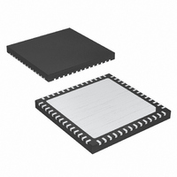
MAX19713ETN+ Maxim Integrated Products, MAX19713ETN+ Datasheet - Page 20

MAX19713ETN+
Manufacturer Part Number
MAX19713ETN+
Description
IC ANLG FRONT END 45MSPS 56-TQFN
Manufacturer
Maxim Integrated Products
Datasheet
1.MAX19713ETN.pdf
(37 pages)
Specifications of MAX19713ETN+
Number Of Bits
10
Number Of Channels
2
Power (watts)
91.8mW
Voltage - Supply, Analog
3V
Voltage - Supply, Digital
3V
Package / Case
56-TQFN Exposed Pad
Lead Free Status / RoHS Status
Lead free / RoHS Compliant
10-Bit, 45Msps, Full-Duplex
Analog Front-End
Figure 5 shows the relationship among the clock, input
data, and analog outputs. Channel ID data is latched
on the falling edge of the clock signal, and channel QD
data is latched on the rising edge of the clock signal, at
which point both ID and QD outputs are simultaneously
updated.
The 3-wire serial interface controls the MAX19713 oper-
ation modes as well as the three 12-bit aux-DACs and
the 10-bit aux-ADC. Upon power-up, program the
MAX19713 to operate in the desired mode. Use the 3-
wire serial interface to program the device for shutdown,
idle, standby, FD, Rx, Tx, aux-DAC controls, or aux-ADC
conversion. A 16-bit data register sets the mode control
as shown in Table 3. The 16-bit word is composed of
four control bits (A3–A0) and 12 data bits (D11–D0).
Data is shifted in MSB first (D11) and LSB last (A0) for-
mat. Table 4 shows the MAX19713 power-management
modes. Table 5 shows the SPI-controlled Tx, Rx, and FD
modes. The serial interface remains active in all modes.
Program the control bits, A3–A0, in the register as shown
in Table 3 to select the operating mode. Modify A3–A0
bits to select from ENABLE-16, Aux-DAC1, Aux-DAC2,
Aux-DAC3, IOFFSET, QOFFSET, COMSEL, Aux-ADC,
ENABLE-8, and WAKEUP-SEL modes. ENABLE-16 is
the default operating mode (see Table 6). This mode
allows for shutdown, idle, and standby states as well as
switching between FAST, SLOW, Rx and Tx modes. Tables
4 and 5 show the required SPI settings for each mode.
In ENABLE-16 mode, the aux-DACs have independent
control bits E4, E5, and E6, bit E9 enables the aux-ADC.
Table 7 shows the auxiliary DAC enable codes. Table 8
shows the auxiliary ADC enable code. Bits E11 and E10
are reserved. Program bits E11 and E10 to logic-low.
Bits E3, E7, and E8 are not used.
Modes aux-DAC1, aux-DAC2, and aux-DAC3 select the
aux-DAC channels named DAC1, DAC2, and DAC3 and
hold the data inputs for each DAC. Bits _D11–_D0 are
the data inputs for each aux-DAC and can be pro-
grammed through SPI. The MAX19713 also includes
two 6-bit registers that can be programmed to adjust the
offsets for the Tx DAC ID and QD channels indepen-
dently (see Table 9). Use the COMSEL mode to select
the output common-mode voltage with bits CM1 and
CM0 (see Table 10). Use aux-ADC mode to start the
auxiliary ADC conversion (see the 10-Bit, 333ksps
Auxiliary ADC section for details). Use ENABLE-8 mode
20
______________________________________________________________________________________
3-Wire Serial Interface and
SPI Register Description
Operation Modes
Tx DAC Timing
for faster enable and switching between shutdown, idle,
and standby states as well as switching between FAST,
SLOW, Rx and Tx modes and the FD mode.
The WAKEUP-SEL register selects the operating mode
that the MAX19713 is to enter immediately after coming
out of shutdown (Table 11). See the Wake-Up Function
section for more information.
Shutdown mode offers the most dramatic power savings
by shutting down all the analog sections (including the
reference) of the MAX19713. In shutdown mode, the Rx
ADC digital outputs are in tri-state mode, the Tx DAC
digital inputs are internally pulled to OV
DAC outputs are at 0V. When the Rx ADC outputs transi-
tion from tri-state to active mode, the last converted word
is placed on the digital output bus. The Tx DAC previ-
ously stored data is lost when coming out of shutdown
mode. The wake-up time from shutdown mode is domi-
nated by the time required to charge the capacitors at
REFP, REFN, and COM. In internal reference mode and
buffered external reference mode, the wake-up time is
typically 500µs to enter Rx mode, 26.4µs to enter Tx
mode, and 500µs to enter FD mode.
In all operating modes, the Tx DAC inputs DA0–DA9 are
internally pulled to OV
the MAX19713 in shutdown mode do not pull DA0–DA9
low. This consideration is especially important in shut-
down mode to achieve the lowest quiescent current.
In idle mode, the reference and clock distribution cir-
cuits are powered, but all other functions are off. The
Rx ADC outputs AD0–AD9 are forced to tri-state. The
Tx DAC DA0–DA9 inputs are internally pulled to OV
while the Tx DAC outputs are at 0V. The wake-up time
is 3.7µs to enter Rx mode, 5.1µs to enter Tx mode, and
5.1µs to enter FD mode. When the Rx ADC outputs
transition from tri-state to active, the last converted
word is placed on the digital output bus.
In standby mode, the reference is powered but all other
device functions are off. The wake-up time from stand-
by mode is 3.8µs to enter Rx mode, 24.4µs to enter Tx
mode, and 24.4µs to enter FD mode. When the Rx ADC
outputs transition from tri-state to active, the last con-
verted word is placed on the digital output bus.
The MAX19713 features FAST and SLOW modes for
switching between Rx and Tx operation. In FAST Tx
mode, the Rx ADC core is powered on but the ADC digi-
tal outputs AD0–AD9 are tri-stated. The Tx DAC digital
bus is active and the DAC core is fully operational.
FAST and SLOW Rx and Tx Modes
DD
. To reduce the supply current of
DD
, and the Tx
DD
,


