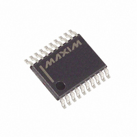
DS1306EN Maxim Integrated Products, DS1306EN Datasheet - Page 13

DS1306EN
Manufacturer Part Number
DS1306EN
Description
IC RTC SERIAL ALARM IND 20-TSSOP
Manufacturer
Maxim Integrated Products
Type
Clock/Calendar/Alarmr
Datasheet
1.DS1306E.pdf
(22 pages)
Specifications of DS1306EN
Memory Size
96B
Time Format
HH:MM:SS (12/24 hr)
Date Format
YY-MM-DD-dd
Interface
SPI, 3-Wire Serial
Voltage - Supply
2 V ~ 5.5 V
Operating Temperature
-40°C ~ 85°C
Mounting Type
Surface Mount
Package / Case
20-TSSOP
Lead Free Status / RoHS Status
Contains lead / RoHS non-compliant
Available stocks
Company
Part Number
Manufacturer
Quantity
Price
Part Number:
DS1306EN
Manufacturer:
MAXIM/美信
Quantity:
20 000
Company:
Part Number:
DS1306EN+
Manufacturer:
Maxim
Quantity:
3 844
Company:
Part Number:
DS1306EN+
Manufacturer:
AD
Quantity:
5 412
Part Number:
DS1306EN+
Manufacturer:
MAXIM/美信
Quantity:
20 000
Part Number:
DS1306EN+T
Manufacturer:
MAXIM/美信
Quantity:
20 000
Company:
Part Number:
DS1306EN+T&R
Manufacturer:
XILINX
Quantity:
210
Part Number:
DS1306EN+TR
Manufacturer:
MAXIM/美信
Quantity:
20 000
DS1306
Figure 8. SPI MULTIPLE-BYTE BURST TRANSFER
READING AND WRITING IN BURST MODE
Burst mode is similar to a single-byte read or write, except that CE is kept high and additional SCLK
cycles are sent until the end of the burst. The clock registers and the user RAM may be read or written in
burst mode. When accessing the clock registers in burst mode, the address pointer will wrap around after
reaching 1Fh (9Fh for writes). When accessing the user RAM in burst mode, the address pointer wraps
around after reaching 7Fh (FFh for writes).
3-WIRE INTERFACE
The 3-wire interface mode operates similar to the SPI mode. However, in 3-wire mode there is one I/O
instead of separate data in and data out signals. The 3-wire interface consists of the I/O (SDI and SDO
pins tied together), CE, and SCLK pins. In 3-wire mode, each byte is shifted in LSB first, unlike SPI
mode, where each byte is shifted in MSB first.
As is the case with the SPI mode, an address byte is written to the device followed by a single data byte
or multiple data bytes. Figure 9 illustrates a read and write cycle. In 3-wire mode, data is input on the
rising edge of SCLK and output on the falling edge of SCLK.
13 of 22


