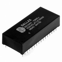
DS1556W-120IND+ Maxim Integrated Products, DS1556W-120IND+ Datasheet - Page 4

DS1556W-120IND+
Manufacturer Part Number
DS1556W-120IND+
Description
IC RTC RAM Y2K 3.3V 120NS 32EDIP
Manufacturer
Maxim Integrated Products
Type
Clock/Calendar/NVSRAM/Y2Kr
Datasheet
1.DS1556P-70.pdf
(18 pages)
Specifications of DS1556W-120IND+
Memory Size
1M (128K x 8)
Time Format
HH:MM:SS (24 hr)
Date Format
YY-MM-DD-dd
Interface
Parallel
Voltage - Supply
3 V ~ 3.6 V
Operating Temperature
-40°C ~ 85°C
Mounting Type
Through Hole
Package / Case
32-DIP Module (600 mil), 32-EDIP
Lead Free Status / RoHS Status
Lead free / RoHS Compliant
Figure 1. Block Diagram
Table 1. Operating Modes
DATA READ MODE
The DS1556 is in the read mode whenever CE (chip enable) is low and WE (write enable) is high. The
device architecture allows ripple-through access to any valid address location. Valid data will be available
at the DQ pins within t
satisfied. If CE or OE access times are not met, valid data will be available at the latter of chip enable
access (t
controlled by CE and OE. If the outputs are activated before t
intermediate state until t
will remain valid for output data hold time (t
access.
DATA WRITE MODE
The DS1556 is in the write mode whenever WE and CE are in their active state. The start of a write is
referenced to the latter occurring transition of WE or CE. The addresses must be held valid throughout the
cycle. CE and WE must return inactive for a minimum of t
or write cycle. Data in must be valid t
V
V
SO
CC
V
< V
<V
CC
V
CEA
> V
CC
SO
CC
) or at output enable access time (t
< V
<V
PF
PF
PF
V
CE
V
V
V
X
X
AA
IH
IL
IL
IL
AA
after the last address input is stable, providing that CE and OE access times are
. If the address inputs are changed while CE and OE remain valid, output data
V
V
OE
X
X
X
X
IL
IH
WE
V
V
V
X
X
X
IH
IH
IL
DS
prior to the end of the write and remain valid for t
DQ0–DQ7
High-Z
High-Z
High-Z
High-Z
D
OH)
D
OUT
4 of 18
IN
OEA
DS1556 1M, Nonvolatile, Y2K-Compliant Timekeeping RAM
but will then go indeterminate until the next address
). The state of the data input/output pins (DQ) is
WR
Data Retention
prior to the initiation of a subsequent read
Deselect
Deselect
MODE
Write
Read
Read
AA
, the data lines are driven to an
CMOS Standby
Battery Current
POWER
Standby
Active
Active
Active
DS1556
DH
Maxim
afterward. In


