DS1644-120+ Maxim Integrated Products, DS1644-120+ Datasheet - Page 5
DS1644-120+
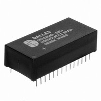
Manufacturer Part Number
DS1644-120+
Description
IC RAM TIMEKEEP NV 120NS 28-EDIP
Manufacturer
Maxim Integrated Products
Type
Clock/Calendar/NVSRAMr
Datasheet
1.DS1644P-120.pdf
(14 pages)
Specifications of DS1644-120+
Memory Size
256K (32K x 8)
Time Format
HH:MM:SS (24 hr)
Date Format
YY-MM-DD-dd
Interface
Parallel
Voltage - Supply
4.5 V ~ 5.5 V
Operating Temperature
0°C ~ 70°C
Mounting Type
Through Hole
Package / Case
28-DIP Module (600 mil), 28-EDIP
Function
Clock/Calendar/NV Timekeeping RAM
Rtc Memory Size
32768 Byte
Supply Voltage (max)
5.5 V
Supply Voltage (min)
4.5 V
Maximum Operating Temperature
+ 70 C
Minimum Operating Temperature
0 C
Mounting Style
Through Hole
Rtc Bus Interface
Parallel
Lead Free Status / RoHS Status
Lead free / RoHS Compliant


DS1644 REGISTER MAP—BANK1 Table 2
OSC = STOP BIT
W = WRITE BIT
Note: All indicated “X” bits are unused but must be set to “0” during write cycles to ensure proper clock
operation.
RETRIEVING DATA FROM RAM OR CLOCK
The DS1644 is in the read mode whenever
device architecture allows ripple-through access to any of the address locations in the NV SRAM. Valid
data will be available at the DQ pins within t
and
available at the latter of chip enable access (t
data input/output pins (DQ) is controlled by
lines are driven to an intermediate state until t
remain valid, output data will remain valid for output data hold time (t
until the next address access.
WRITING DATA TO RAM OR CLOCK
The DS1644 is in the write mode whenever
referenced to the latter occurring high to low transition of
throughout the cycle.
another read or write cycle. Data in must be valid t
afterward. In a typical application, the
active provided that care is taken with the data bus to avoid bus contention. If
transitioning low the data bus can become active with read data defined by the address inputs. A low
transition on
ADDRESS
7FFD
7FFA
7FFC
7FFB
7FFF
7FFE
7FF9
7FF8
OE
access times and states are satisfied. If
WE
OSC
B
—
W
X
X
X
X
X
will then disable the outputs t
7
R = READ BIT
X = UNUSED
CE
FT
B
—
—
—
X
X
X
R
6
or
WE
B
—
—
—
—
X
X
X
-
5
must return inactive for a minimum of t
FT = FREQUENCY TEST
OE
B
—
—
—
—
—
—
X
X
signal will be high during a write cycle. However,
DATA
4
WE
AA
CE
WE
CEA
WEZ
after the last address input is stable, providing that the
AA
(write enable) is high, and
) or at output enable access time (t
and
CE
5 of 14
. If the address inputs are changed while
and
B
—
—
—
—
—
—
X
X
after
3
DS
or
OE
CE
prior to the end of write and remain valid for t
OE
WE
. If the outputs are activated before t
B
—
—
—
—
—
—
—
are in their active state. The start of a write is
X
WE
2
access times are not met, valid data will be
goes active.
or
CE
B
—
—
—
—
—
—
—
X
1
. The addresses must be held valid
OH
) but will then go indeterminate
B
—
—
—
—
—
—
—
X
CE
WR
0
(chip enable) is low. The
prior to the initiation of
OE
Seconds
Minutes
Control
Month
OEA
Hour
Year
Date
Day
is low prior to
FUNCTION
). The state of the
DS1644/DS1644P
CE
AA
OE
, the data
00-99
01-12
01-31
01-07
00-23
00-59
00-59
and
A
can be
WE
CE
OE
DH
Related parts for DS1644-120+
Image
Part Number
Description
Manufacturer
Datasheet
Request
R

Part Number:
Description:
IC RAM TIMEKEEP NV 120NS 28-EDIP
Manufacturer:
Maxim Integrated Products
Datasheet:

Part Number:
Description:
MAX7528KCWPMaxim Integrated Products [CMOS Dual 8-Bit Buffered Multiplying DACs]
Manufacturer:
Maxim Integrated Products
Datasheet:
Part Number:
Description:
Single +5V, fully integrated, 1.25Gbps laser diode driver.
Manufacturer:
Maxim Integrated Products
Datasheet:
Part Number:
Description:
Single +5V, fully integrated, 155Mbps laser diode driver.
Manufacturer:
Maxim Integrated Products
Datasheet:
Part Number:
Description:
VRD11/VRD10, K8 Rev F 2/3/4-Phase PWM Controllers with Integrated Dual MOSFET Drivers
Manufacturer:
Maxim Integrated Products
Datasheet:
Part Number:
Description:
Highly Integrated Level 2 SMBus Battery Chargers
Manufacturer:
Maxim Integrated Products
Datasheet:
Part Number:
Description:
Current Monitor and Accumulator with Integrated Sense Resistor; ; Temperature Range: -40°C to +85°C
Manufacturer:
Maxim Integrated Products
Part Number:
Description:
TSSOP 14/A�/RS-485 Transceivers with Integrated 100O/120O Termination Resis
Manufacturer:
Maxim Integrated Products
Part Number:
Description:
TSSOP 14/A�/RS-485 Transceivers with Integrated 100O/120O Termination Resis
Manufacturer:
Maxim Integrated Products
Part Number:
Description:
QFN 16/A�/AC-DC and DC-DC Peak-Current-Mode Converters with Integrated Step
Manufacturer:
Maxim Integrated Products
Part Number:
Description:
TDFN/A/65V, 1A, 600KHZ, SYNCHRONOUS STEP-DOWN REGULATOR WITH INTEGRATED SWI
Manufacturer:
Maxim Integrated Products
Part Number:
Description:
Integrated Temperature Controller f
Manufacturer:
Maxim Integrated Products
Part Number:
Description:
SOT23-6/I�/45MHz to 650MHz, Integrated IF VCOs with Differential Output
Manufacturer:
Maxim Integrated Products
Part Number:
Description:
SOT23-6/I�/45MHz to 650MHz, Integrated IF VCOs with Differential Output
Manufacturer:
Maxim Integrated Products
Part Number:
Description:
EVALUATION KIT/2.4GHZ TO 2.5GHZ 802.11G/B RF TRANSCEIVER WITH INTEGRATED PA
Manufacturer:
Maxim Integrated Products