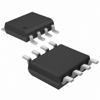
DS1340Z-33+ Maxim Integrated Products, DS1340Z-33+ Datasheet - Page 10

DS1340Z-33+
Manufacturer Part Number
DS1340Z-33+
Description
IC RTC I2C W/CHARGER 3.3V 8-SOIC
Manufacturer
Maxim Integrated Products
Type
Clock/Calendar/Trickle-Chargerr
Datasheet
1.DS1340U-33.pdf
(16 pages)
Specifications of DS1340Z-33+
Time Format
HH:MM:SS (24 hr)
Date Format
YY-MM-DD-dd
Interface
I²C, 2-Wire Serial
Voltage - Supply
2.97 V ~ 5.5 V
Operating Temperature
-40°C ~ 85°C
Mounting Type
Surface Mount
Package / Case
8-SOIC (3.9mm Width)
Function
Clock/Calendar/Trickle Charger
Supply Voltage (max)
5.5 V
Supply Voltage (min)
2.97 V
Maximum Operating Temperature
+ 85 C
Minimum Operating Temperature
- 40 C
Mounting Style
SMD/SMT
Rtc Bus Interface
Serial (I2C)
Supply Current
192 uA
Lead Free Status / RoHS Status
Lead free / RoHS Compliant
Memory Size
-
Lead Free Status / Rohs Status
Lead free / RoHS Compliant
pattern on 1010 enables the trickle charger. All other
patterns disable the trickle charger. The trickle charger
is disabled when power is first applied. The diode-
select (DS) bits (bits 2, 3) select whether or not a diode
is connected between V
no diode is selected; if DS is 10, a diode is selected.
The ROUT bits (bits 0, 1) select the value of the resistor
connected between V
the resistor selected by the resistor select (ROUT) bits
and the diode selected by the diode select (DS) bits.
Warning: The ROUT value of 250Ω must not be select-
ed whenever V
The user determines diode and resistor selection
according to the maximum current desired for battery
or super cap charging (Table 4). The maximum charg-
ing current can be calculated as illustrated in the fol-
lowing example.
Assume that a 3.3V system power supply is applied to
V
assume that the trickle charger has been enabled with
a diode and resistor R2 between V
The maximum current I
ed as follows:
As the super cap charges, the voltage drop between
V
current decreases.
Bit 7: Oscillator Stop Flag (OSF). A logic 1 in this bit
indicates that the oscillator has stopped or was
stopped for some time period and may be used to
judge the validity of the clock and calendar data. This
bit is edge triggered and is set to logic 1 when the
I
Table 4. Trickle-Charge Register
10
CC
CC
2
TCS3
I
C RTC with Trickle Charger
X
X
X
1
1
1
1
1
1
0
and V
MAX
and a super cap is connected to V
____________________________________________________________________
= (3.3V - diode drop) / R2 ≈ (3.3V - 0.7V) /
BACKUP
TCS2
CC
X
X
X
0
0
0
0
0
0
0
is greater than 3.63V.
decreases and therefore the charge
2kΩ ≈ 1.3mA
CC
MAX
CC
TCS1
and V
X
X
X
1
1
1
1
1
1
0
would therefore be calculat-
and V
Flag Register (09h)
BACKUP
BACKUP
TCS0
CC
X
X
X
0
0
0
0
0
0
0
. Table 3 shows
and V
BACKUP
. If DS is 01,
BACKUP
DS1
X
0
1
0
1
0
1
0
1
0
. Also
.
DS0
0
1
X
1
0
1
0
1
0
0
internal circuitry senses that the oscillator has transi-
tioned from a normal run state to a STOP condition. The
following are examples of conditions that can cause the
OSF bit to be set:
The OSF bit remains at logic 1 until written to logic 0. It
can only be written to logic 0. Attempting to write OSF
to logic 1 leaves the value unchanged.
Bits 6 to 0: All other bits in the flag register read as 0
and cannot be written.
The DS1340 provides a digital clock calibration feature
to allow compensation for crystal and temperature vari-
ations. The calibration circuit adds or subtracts counts
from the oscillator divider chain at the divide-by-256
stage. The number of pulses blanked (subtracted for
negative calibration) or inserted (added for positive cal-
ibration) depends upon the value loaded into the five
calibration bits (CAL4–CAL0) located in the control reg-
ister. Adding counts speeds the clock up and subtract-
ing counts slows the clock down.
The calibration bits can be set to any value between 0
and 31 in binary form. Bit 5 of the control register, S, is
the sign bit. A value of 1 for the S bit indicates positive
calibration, while a value of 0 represents negative cali-
bration. Calibration occurs within a 64-minute cycle.
The first 62 minutes in the cycle can, once per minute,
1)
2)
3)
4)
ROUT1
The first time power is applied.
The voltages present on V
are insufficient to support oscillation.
The EOSC bit is set to 1, disabling the
oscillator.
External influences on the crystal (e.g., noise,
leakage).
X
X
0
0
0
1
1
1
1
0
ROUT0
X
X
0
1
1
0
0
1
1
0
Clock Calibration
Disabled
Disabled
Disabled
No diode, 250Ω resistor
One diode, 250Ω resistor
No diode, 2kΩ resistor
One diode, 2kΩ resistor
No diode, 4kΩ resistor
One diode, 4kΩ resistor
Power-on reset value
FUNCTION
CC
and V
BACKUP


