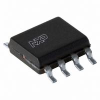
PCF8593T/1,112 NXP Semiconductors, PCF8593T/1,112 Datasheet - Page 14

PCF8593T/1,112
Manufacturer Part Number
PCF8593T/1,112
Description
IC CLOCK/CALENDAR LOW PWR 8-SOIC
Manufacturer
NXP Semiconductors
Type
Clock/Calendar/NVSRAMr
Datasheet
1.PCF8593T1118.pdf
(35 pages)
Specifications of PCF8593T/1,112
Package / Case
8-SOIC (3.9mm Width)
Time Format
HH:MM:SS:hh (12/24 hr)
Memory Size
8B
Date Format
YY-MM-DD-dd
Interface
I²C, 2-Wire Serial
Voltage - Supply
1 V ~ 6 V
Operating Temperature
-40°C ~ 85°C
Mounting Type
Surface Mount
Function
Clock, Calendar, Alarm, Timer Interrupt
Rtc Memory Size
8 B
Supply Voltage (max)
6 V
Supply Voltage (min)
1 V
Maximum Operating Temperature
+ 85 C
Minimum Operating Temperature
- 40 C
Mounting Style
SMD/SMT
Rtc Bus Interface
Serial
Lead Free Status / RoHS Status
Lead free / RoHS Compliant
Other names
935275723112
PCF8593TD
PCF8593TD
PCF8593TD
PCF8593TD
Available stocks
Company
Part Number
Manufacturer
Quantity
Price
Part Number:
PCF8593T/1,112
Manufacturer:
NXP/恩智浦
Quantity:
20 000
NXP Semiconductors
8. Characteristics of the I
PCF8593
Product data sheet
8.1.1 Bit transfer
8.1.2 Start and stop conditions
8.1.3 System configuration
8.1 Characteristics
The I
The two lines are a Serial DAta line (SDA) and a Serial Clock Line (SCL). Both lines must
be connected to a positive supply via a pull-up resistor. Data transfer is initiated only when
the bus is not busy.
One data bit is transferred during each clock pulse (see
line must remain stable during the HIGH period of the clock pulse as changes in the data
line at this time are interpreted as a control signal.
Both data and clock lines remain HIGH when the bus is not busy.
A HIGH-to-LOW transition of the data line while the clock is HIGH is defined as the START
condition - S.
A LOW-to-HIGH transition of the data line while the clock is HIGH is defined as the STOP
condition - P (see
A device generating a message is a transmitter; a device receiving a message is the
receiver (see
devices which are controlled by the master are the slaves.
Fig 14. Bit transfer
Fig 15. Definition of start and stop conditions
2
C-bus is for bidirectional, two-line communication between different ICs or modules.
SDA
SCL
Figure
START condition
All information provided in this document is subject to legal disclaimers.
2
SDA
SCL
Figure
C-bus
S
16). The device that controls the message is the master; and the
Rev. 04 — 6 October 2010
15).
data valid
data line
stable;
allowed
change
of data
Figure
Low power clock and calendar
STOP condition
14). The data on the SDA
mbc621
P
PCF8593
© NXP B.V. 2010. All rights reserved.
mbc622
SDA
SCL
14 of 35


