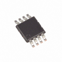
DS1371U+ Maxim Integrated Products, DS1371U+ Datasheet - Page 10

DS1371U+
Manufacturer Part Number
DS1371U+
Description
IC BINARY COUNTER 32-BIT 8-USOP
Manufacturer
Maxim Integrated Products
Type
Binary Counterr
Datasheet
1.DS1371U.pdf
(15 pages)
Specifications of DS1371U+
Time Format
Binary
Date Format
Binary
Interface
I²C, 2-Wire Serial
Voltage - Supply
1.7 V ~ 5.5 V
Operating Temperature
-40°C ~ 85°C
Mounting Type
Surface Mount
Package / Case
8-MSOP, Micro8™, 8-uMAX, 8-uSOP,
Counter Type
Binary Counters
Number Of Bits
32
Operating Temperature Range
- 40 C to + 85 C
Mounting Style
SMD/SMT
Clock Frequency
400kHz
Supply Voltage Range
1.7V To 5.5V
No. Of Pins
8
Clock Format
Binary
Rohs Compliant
Yes
Lead Free Status / RoHS Status
Lead free / RoHS Compliant
Memory Size
-
Lead Free Status / Rohs Status
Lead free / RoHS Compliant
Bit #
Name
Default
Special Purpose Registers
The DS1371 has two additional registers (07h–08h) that control the WD/ALM counter, square-wave
output, and interrupts.
Control Register (07h)
Bit 7: Enable Oscillator (EOSC). When set to logic 0, the oscillator is started. When set to logic 1, the
oscillator is stopped. When this bit is set to a logic 1, the oscillator is stopped and the DS1371 is placed
into a low-power standby mode (I
Bit 6: WD/ALM Counter Enable (WACE). When set to logic 1, the WD/ALM counter is enabled.
When set to logic 0, the WD/ALM counter is disabled, and the 24-bits can be used as general-purpose
RAM. This bit is clear (logic 0) when power is first applied.
Bit 5: WD/ALM Counter Select (WD/ALM). When set to logic 0, the counter decrements every second
until it reaches 0 and is then reloaded and restarted. When set to logic 1, the WD/ALM counter
decrements every 1/4096 of a second (approximately every 244μs) until it reaches 0, sets the AF bit in the
status register, and stops. If any of the WD/ALM counter registers are read or written, or a rising edge on
the WDS pin occurs before the counter reaches 0, the counter is reloaded and restarted. This bit is clear
(logic 0) when power is first applied.
Bit 3: Interrupt Control (INTCN). This bit controls the SQW/INT signal. When the INTCN bit is set to
logic 0, a square wave is output on the SQW/INT pin whose frequency is defined by bits RS2 and RS1.
The oscillator must also be enabled for the square wave to be output. When the INTCN bit is set to logic
1, then this permits the alarm flag bit in the status register to assert SQW/INT (provided that the alarm is
also enabled). The alarm flag is always set, regardless of the state of the INTCN bit. The INTCN bit is set
to logic 0 when power is first applied.
Bits 2 and 1: Rate Select 1 and 2 (RS2 and RS1). These bits control the frequency of the square-wave
output when the square wave has been enabled. Table 3 shows the square-wave frequencies that can be
selected with the RS bits. These bits are both set (logic 1) when power is first applied.
Bit 0: Alarm Interrupt Enable (AIE). When set to logic 1, this bit permits the AF bit in the status
register to assert SQW/INT (when INTCN = 1). When set to logic 0 or INTCN is set to logic 0, the AF bit
does not initiate the SQW/INT signal. If the WD/ALM bit is set to a logic 1 and the AF flag is set, writing
AIE to a 0 does not truncate the 250ms pulse on the SQW/INT pin. The AIE bit is at logic 0 when power
is first applied.
Table 3. SQW/INT Operating Modes
WACE
X
X
X
X
1
1
WD/ALM
EOSC
7
0
X
X
X
X
0
1
WACE
INTCN
6
0
0
0
0
0
1
1
DDR
). This bit is clear (logic 0) when power is first applied.
WD/ALM
AIE
X
X
X
X
5
0
1
1
10 of 15
RS2
X
X
0
0
1
1
4
0
0
INTCN
RS1
X
X
0
1
0
1
3
0
SQW/INT OUTPUT
RS2
2
1
32.768kHz
4.096kHz
8.192kHz
Alarm
1Hz
WD
RS1
1
1
AIE
0
0


