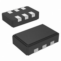
CY2XF33FLXCT Cypress Semiconductor Corp, CY2XF33FLXCT Datasheet - Page 4

CY2XF33FLXCT
Manufacturer Part Number
CY2XF33FLXCT
Description
IC XTAL OSC CMOS 6CLCC
Manufacturer
Cypress Semiconductor Corp
Specifications of CY2XF33FLXCT
Pll
Yes
Input
Crystal
Output
LVDS
Number Of Circuits
1
Ratio - Input:output
1:1
Differential - Input:output
No/Yes
Frequency - Max
690MHz
Divider/multiplier
Yes/No
Voltage - Supply
*
Operating Temperature
*
Mounting Type
Surface Mount
Package / Case
6-CLCC
Frequency
*
Count
*
Operating Supply Voltage (typ)
2.5/3.3
Output Level
LVDS
Symmetry Max
60%
Operating Temp Range
0C to 70C
Screening Level
Commercial
Lead Free Status / RoHS Status
Lead free / RoHS Compliant
Application-Specific Factory Configurations
Programming Variables
Output Frequencies
The CY2XF33 is programmed with up to four independent output
frequencies, which are then selected using the FS0 and FS1
pins. The device can synthesize frequencies to a resolution of 1
part per million (ppm), but the actual accuracy of the output
frequency is limited by the accuracy of the integrated reference
crystal.
The CY2XF33 has an output frequency range of 50 MHz to
690 MHz, but the range is not continuous. The CY2XF33 cannot
generate frequencies in the ranges of 521 MHz to 529 MHz and
596 MHz to 617 MHz.
Industrial Versus Commercial Device Performance
Industrial and Commercial devices have different internal
crystals. This has a potentially significant impact on performance
levels for applications requiring the lowest possible phase noise.
CyberClocks Online Software displays expected performance
for both options.
Phase Noise Versus Jitter Performance
In most cases, the device configuration for optimal phase noise
performance is different from the device configuration for optimal
cycle to cycle or period jitter. CyberClocks Online Software
includes algorithms to optimize performance for either
parameter.
Document Number: 001-53148 Rev. *D
CY2XF33LXC533T
CY2XF33LXC700T
Part Number
2.5 V
3.3 V
VDD
FS1
0
0
1
1
0
0
1
1
FS0
0
1
0
1
0
1
0
1
Output Frequency
350.00 MHz
533.00 MHz
400.00 MHz
200.00 MHz
100.00 MHz
125.00 MHz
200.00 MHz
250.00 MHz
Table 3. Device Programming Variables
Output frequency 0 (Power on default)
Output frequency 1
Output frequency 2
Output frequency 3
Optimization (phase noise or jitter)
Temperature range (Commercial or industrial)
12 kHz to 20 MHz
12 kHz to 20 MHz
Offset Range
RMS Phase Jitter (Random)
Variable
Jitter (Typical)
0.51 ps
1.00 ps
0.49 ps
0.55 ps
0.65 ps
0.61 ps
0.55 ps
0.53 ps
CY2XF33
Page 4 of 11
[+] Feedback


