NB3N5573DTG ON Semiconductor, NB3N5573DTG Datasheet
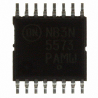
IC CLOCK GEN XTAL - HCSL 16TSSOP

NB3N5573DTG

Manufacturer Part Number
NB3N5573DTG
Description
IC CLOCK GEN XTAL - HCSL 16TSSOP
Manufacturer
ON Semiconductor
Type
Clock Generatorr
Datasheet

Specifications of NB3N5573DTG

Pll
Yes
Input
Clock, Crystal
Output
HCSL
Number Of Circuits
1
Ratio - Input:output
1:2
Differential - Input:output
No/Yes
Frequency - Max
200MHz
Divider/multiplier
Yes/No
Voltage - Supply
2.97 V ~ 3.63 V
Operating Temperature
-40°C ~ 85°C
Mounting Type
Surface Mount
Package / Case
16-TSSOP
Frequency-max
200MHz
Number Of Elements
1
Supply Current
135mA
Pll Input Freq (min)
25MHz
Operating Supply Voltage (typ)
3.3V
Operating Temp Range
-40C to 85C
Package Type
TSSOP
Output Frequency Range
25 to 200MHz
Operating Supply Voltage (min)
2.97V
Operating Supply Voltage (max)
3.63V
Operating Temperature Classification
Industrial
Pin Count
16
Lead Free Status / RoHS Status
Lead free / RoHS Compliant
Other names
NB3N5573DTGOS

Available stocks

Company
Part Number
Manufacturer
Quantity
Price
Part Number:
NB3N5573DTG
Manufacturer:
ON
Quantity:
96
Part Number:
NB3N5573DTG
Manufacturer:
ON Semiconductor
Quantity:
52
Part Number:
NB3N5573DTG
Manufacturer:
ON/安森美
Quantity:
20 000
NB3N5573
3.3V, Crystal-to-HCSL
Clock Generator
Description
that supports PCI Express and Ethernet requirements. The device
takes a 25 MHz fundamental mode parallel resonant crystal and
generates differential HCSL output at 25 MHz, 100 MHz, 125 MHz or
200 MHz clock frequencies. Outputs can interface with LVDS with
proper termination (See Figure 4).
pin package.
Features
© Semiconductor Components Industries, LLC, 2010
June, 2010 − Rev. 3
The NB3N5573 is a high precision, low phase noise clock generator
This device is housed in 5.0 mm x 4.4 mm narrow body TSSOP 16
Uses 25 MHz Fundamental Mode Parallel Resonant Crystal
External Loop Filter is Not Required
HCSL Differential Output or LVDS with Proper Termination
Phase Noise:
Typical Period Jitter RMS of 1.5 ps
Operating Range 3.3 V ±10%
Industrial Temperature Range −40°C to +85°C
These are Pb−Free Devices
25 MHz Clock or
Offset
100 Hz
1 kHz
10 kHz
100 kHz
1 MHz
10 MHz
Crystal
X1/CLK
Noise Power
−103 dBc/Hz
−118 dBc/Hz
−122 dBc/Hz
−130 dBc/Hz
−132 dBc/Hz
−149 dBc/Hz
X2
Crystal Oscillator
Clock Buffer
VDD
Figure 1. NB3N5573 Simplified Logic Diagram
GND
Detector
Phase
BN
1
Charge
Pump
See detailed ordering and shipping information in the package
dimensions section on page 5 of this data sheet.
16
(Note: Microdot may be in either location)
S0
CASE 948F
DT SUFFIX
TSSOP−16
A
L
Y
W
G
VCO
ORDERING INFORMATION
http://onsemi.com
1
S1
= Assembly Location
= Wafer Lot
= Year
= Work Week
= Pb−Free Package
Publication Order Number:
OE
Output
Output
HSCL
HSCL
16
IREF
1
MARKING
DIAGRAM
ALYWG
NB3N
5573
NB3N5573/D
G
CLK0
CLK0
CLK1
CLK1

Related parts for NB3N5573DTG

NB3N5573DTG Summary of contents

Page 1

NB3N5573 3.3V, Crystal-to-HCSL Clock Generator Description The NB3N5573 is a high precision, low phase noise clock generator that supports PCI Express and Ethernet requirements. The device takes a 25 MHz fundamental mode parallel resonant crystal and generates differential HCSL output ...

Page 2

X1/CLK X2 OE GND NC Table 1. PIN DESCRIPTION Pin Symbol I Input LVTTL/LVCMOS frequency select input 0. Internal pullup resistor to V table 2 for details Input LVTTL/LVCMOS frequency select input 1. ...

Page 3

Table 3. ATTRIBUTES ESD Protection Moisture Sensitivity, Indefinite Time Out of Dray Pack (Note 1) Flammability Rating Transistor Count Meets or exceeds JEDEC Spec EIA/JESD78 IC Latchup Test 1. For additional information, see Application Note AND8003/D. Table 4. MAXIMUM RATINGS ...

Page 4

Table 6. AC CHARACTERISTICS (V DD Symbol f Clock/Crystal Input Frequency CLKIN f Output Clock Frequency CLKOUT W Phase−Noise Performance NOISE T Period Jitter Peak−to−Peak (Note 6) jitter Period Jitter RMS (Note 6) Cycle−Cycle RMS Jitter (Note 7) Cycle−to−Cycle Peak ...

Page 5

... Figure 4. Typical Termination for LVDS Device Load 700 Figure 5. HCSL Output Parameter Characteristics ORDERING INFORMATION Device NB3N5573DTG NB3N5573DTR2G †For information on tape and reel specifications, including part orientation and tape sizes, please refer to our Tape and Reel Packaging Specifications Brochure, BRD8011/ 100 W ...

Page 6

... −V− C 0.10 (0.004) −T− SEATING D PLANE 16X 0.36 *For additional information on our Pb−Free strategy and soldering details, please download the ON Semiconductor Soldering and Mounting Techniques Reference Manual, SOLDERRM/D. PACKAGE DIMENSIONS TSSOP−16 CASE 948F−01 ISSUE Ç Ç Ç ...

Page 7

... Opportunity/Affirmative Action Employer. This literature is subject to all applicable copyright laws and is not for resale in any manner. PUBLICATION ORDERING INFORMATION LITERATURE FULFILLMENT: Literature Distribution Center for ON Semiconductor P.O. Box 5163, Denver, Colorado 80217 USA Phone: 303−675−2175 or 800−344−3860 Toll Free USA/Canada Fax: 303− ...

Related keywords