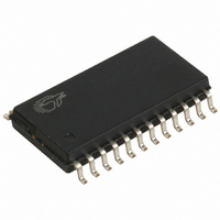
CY7B9920-5SC Cypress Semiconductor Corp, CY7B9920-5SC Datasheet - Page 5

CY7B9920-5SC
Manufacturer Part Number
CY7B9920-5SC
Description
IC CLK BUFF SKEW 8OUT 24SOIC
Manufacturer
Cypress Semiconductor Corp
Type
Fanout Distribution, Zero Delay Bufferr
Datasheet
1.CY7B9920-5SC.pdf
(8 pages)
Specifications of CY7B9920-5SC
Number Of Circuits
1
Package / Case
24-SOIC (7.5mm Width)
Pll
Yes
Input
Clock
Output
CMOS
Ratio - Input:output
1:8
Differential - Input:output
No/No
Frequency - Max
80MHz
Divider/multiplier
No/No
Voltage - Supply
4.5 V ~ 5.5 V
Operating Temperature
0°C ~ 70°C
Mounting Type
Surface Mount
Frequency-max
80MHz
Output Frequency Range
15 MHz to 80 MHz
Supply Voltage (max)
5.5 V
Supply Voltage (min)
4.5 V
Maximum Operating Temperature
+ 70 C
Minimum Operating Temperature
0 C
Mounting Style
SMD/SMT
Operating Supply Voltage
5 V
Lead Free Status / RoHS Status
Contains lead / RoHS non-compliant
Other names
428-1378
Available stocks
Company
Part Number
Manufacturer
Quantity
Price
Part Number:
CY7B9920-5SC
Manufacturer:
CYP
Quantity:
20 000
Company:
Part Number:
CY7B9920-5SCT
Manufacturer:
NICHIA
Quantity:
7 126
Switching Characteristics
t
t
t
Notes:
10. The level to be set on FS is determined by the “normal” operating frequency (f
11. When the FS pin is selected HIGH, the REF input must not transition upon power-up until V
12. Except as noted, all CY7B9920–2 and –5 timing parameters are specified to 80-MHz with a 30-pF load.
13. t
14. t
15. t
16. t
17. Specified with outputs loaded with 30 pF for the CY7B99X0–2 and –5 devices and 50 pF for the CY7B99X0–7 devices. Devices are terminated through 50
18. t
19. t
f
t
t
t
t
t
t
t
t
t
t
t
OFALL
LOCK
JR
7.
8.
9.
NOM
RPWH
RPWL
SKEW
DEV
PD
ODCV
ORISE
OFALL
LOCK
JR
JR
Parameter
Parameter
Test measurement levels for the CY7B9910 are TTL levels (1.5V to 1.5V). Test measurement levels for the CY7B9920 are CMOS levels (V
conditions assume signal transition times of 2ns or less and output loading as shown in the AC Test Loads and Waveforms unless otherwise specified.
Guaranteed by statistical correlation. Tested initially and after any design or process changes that may affect these parameters.
For all three-state inputs, HIGH indicates a connection to V
holds an unconnected input to V
FB inputs will be f
multiplication by using external division in the feedback path of value X.
2.06V (CY7B9910) or V
to 2.06V (CY7B9910) or V
measured from the application of a new signal or frequency at REF or FB until t
SKEW
SKEW
DEV
ODCV
ORISE
LOCK
is the output-to-output skew between any two outputs on separate devices operating under the same conditions (V
is the time that is required before synchronization is achieved. This specification is valid only after V
is the deviation of the output from a 50% duty cycle.
is defined as the skew between outputs.
and t
is defined as the time between the earliest and the latest output transition among all outputs when all are loaded with 50 pF and terminated with 50 to
OFALL
Output Fall Time
PLL Lock Time
Cycle-to-Cycle Output Jitter Peak to Peak
Operating Clock
Frequency in MHz
REF Pulse Width HIGH
REF Pulse Width LOW
Zero Output Skew (All Outputs)
Device-to-Device Skew
Propagation Delay, REF Rise to FB Rise
Output Duty Cycle Variation
Output Rise Time
Output Fall Time
PLL Lock Time
Cycle-to-Cycle Output
Jitter
NOM
measured between 0.8V and 2.0V for the CY7B9910 or 0.8V
when the output connected to FB is undivided. The frequency of the REF and FB inputs will be f
CC
CC
/2 (CY7B9920).
/2 (CY7B9920).
CC
/2.
[19]
[19]
[17, 18]
Description
[17, 18]
Description
[17, 18]
Over the Operating Range
[8, 15]
FS = LOW
FS = MID
FS = HIGH
Peak to Peak
RMS
[16]
RMS
[8]
[13, 14]
[8]
[9, 10]
CC
[9, 10]
[9, 10, 11]
, LOW indicates a connection to GND, and MID indicates an open connection. Internal termination circuitry
[8]
[8]
[7]
PD
CC
(continued)
is within specified limits.
5
and 0.2V
–0.7
–1.2
Min.
0.15
0.15
5.0
5.0
15
25
40
NOM
Min.
0.15
) of the VCO (see Logic Block Diagram). The frequency appearing at the REF and
CY7B9910–7
CC
CY7B9910–5
for the CY7B9920.
Typ.
0.3
0.0
0.0
1.5
1.5
Typ.
1.0
CC
has reached 4.3V.
CC
is stable and within normal operating limits. This parameter is
Max.
0.75
+0.7
+1.2
200
1.5
2.5
2.5
0.5
Max.
30
50
80
25
200
1.5
0.5
25
NOM
CC
, ambient temperature, air flow, etc.).
/X when the device is configured for a frequency
Min.
–0.7
–1.2
5.0
5.0
0.5
0.5
15
25
40
Min.
0.5
CY7B9920–7
CY7B9920–5
Typ.
Typ.
0.3
0.0
0.0
3.0
3.0
2.0
CY7B9910
CY7B9920
80
Max.
+0.7
+1.2
0.75
Max.
200
CC
1.5
5.0
5.0
0.5
200
30
50
25
3.0
0.5
25
[12]
/2 to V
CC
MHz
/2). Test
Unit
Unit
ms
ms
ns
ns
ns
ns
ns
ns
ns
ns
ps
ps
ns
ps
ps


