CY25560SXC Cypress Semiconductor Corp, CY25560SXC Datasheet - Page 2
CY25560SXC
Manufacturer Part Number
CY25560SXC
Description
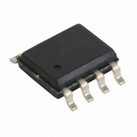
IC CLOCK GEN 3.3V SS 8-SOIC
Manufacturer
Cypress Semiconductor Corp
Type
Clock/Frequency Synthesizer, Frequency Modulator, Spread Spectrum Clock Generatorr
Datasheet
1.CY25560SXC.pdf
(9 pages)
Specifications of CY25560SXC
Number Of Circuits
1
Package / Case
8-SOIC (3.9mm Width)
Pll
Yes
Input
Clock, Crystal
Output
Clock
Ratio - Input:output
1:1
Differential - Input:output
No/No
Frequency - Max
100MHz
Divider/multiplier
Yes/No
Voltage - Supply
2.97 V ~ 3.63 V
Operating Temperature
0°C ~ 70°C
Mounting Type
Surface Mount
Frequency-max
100MHz
Maximum Input Frequency
100 MHz
Minimum Input Frequency
25 MHz
Supply Voltage (max)
3.63 V
Supply Voltage (min)
2.97 V
Maximum Operating Temperature
+ 70 C
Minimum Operating Temperature
0 C
Mounting Style
SMD/SMT
Operating Supply Voltage
3.3 V
Lead Free Status / RoHS Status
Lead free / RoHS Compliant
Lead Free Status / RoHS Status
Lead free / RoHS Compliant, Lead free / RoHS Compliant
Other names
428-2222-5
CY25560SXC
CY25560SXC
Available stocks
Company
Part Number
Manufacturer
Quantity
Price
Company:

Part Number:
CY25560SXC
Manufacturer:
CY
Quantity:
1 262
Part Number:
CY25560SXC
Manufacturer:
CYP
Quantity:
20 000
Company:
Part Number:
CY25560SXCT
Manufacturer:
CYPRESS
Quantity:
1 710
Part Number:
CY25560SXCT
Manufacturer:
CYPRESS/赛普拉斯
Quantity:
20 000


Pinouts
Table 1. Pin Description
General Description
The Cypress CY25560 is a Spread Spectrum Clock Generator
(SSCG) IC used to reduce the EMI found in today’s high-speed
digital electronic systems.
The CY25560 uses Cypress’s proprietary phase-locked loop
(PLL) and Spread Spectrum Clock (SSC) technology to
synthesize and frequency modulate the input frequency of the
reference clock. By frequency modulating the clock, the
measured EMI at the fundamental and harmonic frequencies of
clock (SSCLK) is greatly reduced.
This reduction in radiated energy can significantly reduce the
cost of complying with regulatory requirements and time to
market without degrading system performance.
The CY25560 is a very simple and versatile device to use. The
frequency and spread% range is selected by programming S0
and S1 digital inputs. These inputs use three (3) logic states
including High (H), Low (L) and Middle (M) logic levels to select
one of the nine available spread% ranges. Refer to
programming details.
Document #: 38-07425 Rev. *F
Pin Number Pin Name
1
2
3
4
5
6
7
8
Xin/CLK
SSCLK
SSCC
VDD
GND
Xout
S1
S0
Type
P
P
O
O
I
I
I
I
Clock or Crystal Connection Input. Refer to
Positive Power Supply.
Power Supply Ground.
Modulated Clock Output, which is the Same Frequency as the Input Clock or the Crystal
Frequency.
Spread Spectrum Clock Control (Enable/Disable) FUNCTION. SSCG function is enabled
when input is HIGH and disabled when input is LOW. This pin is pulled HIGH internally.
Tri-level Logic Input Control Pin Used to Select Input Frequency Range and Spread
Percent. Refer to tri-level logic on page 3 for programming details. Pin 6 has an internal resistor
divider network to V
Tri-level Logic Input Control Pin Used to Select Input Frequency Range and Spread
Percent. Refer to tri-level logic on page 3 for programming details. Pin 7 has an internal resistor
divider network to V
Oscillator Output Pin Connected to Crystal. Leave this pin unconnected if an external clock
is used to drive X
Figure 1. Pin Configuration – 8-Pin SOIC Package
XIN/CLK
SSCLK
VDD
VSS
Table 2
IN
/CLK input (Pin 1).
1
2
3
4
DD
DD
and V
and V
for
CY25560
SS
SS
CY25560 is optimized for SVGA (40 MHz) and XVGA (65 MHz)
controller clocks and also suitable for applications where the
frequency range is 25 MHz to 100 MHz.
A wide range of digitally selectable spread percentages is made
possible by using three-level (High, Low, and Middle) logic at the
S0 and S1 digital control inputs.
The output spread (frequency modulation) is symmetrically
centered on the input frequency.
Spread Spectrum Clock Control (SSCC) function enables or
disables the frequency spread and is provided for easy
comparison of system performance during EMI testing.
The CY25560 is available in an 8-pin SOIC package with 0°C to
70°C Commercial and –40°C to 85°C Industrial operating
temperature ranges.
. Refer to
. Refer to
Pin Description
8
7
6
5
Logic Block Diagram
Logic Block Diagram
XOUT
SSCC
S1
S0
Table 2
for input frequency range selection.
on page 1.
on page 1.
CY25560
Page 2 of 9
[+] Feedback
Related parts for CY25560SXC
Image
Part Number
Description
Manufacturer
Datasheet
Request
R

Part Number:
Description:
Manufacturer:
Cypress Semiconductor Corp
Datasheet:
Part Number:
Description:
Manufacturer:
Cypress Semiconductor Corp
Datasheet:
Part Number:
Description:
Manufacturer:
Cypress Semiconductor Corp
Datasheet:
Part Number:
Description:
Manufacturer:
Cypress Semiconductor Corp
Datasheet:
Part Number:
Description:
Manufacturer:
Cypress Semiconductor Corp
Datasheet: