NB6N11SMNG ON Semiconductor, NB6N11SMNG Datasheet - Page 2
NB6N11SMNG
Manufacturer Part Number
NB6N11SMNG
Description
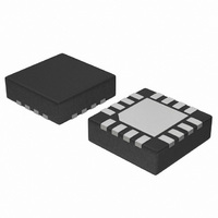
IC BUFFER/XLATOR LVDS 16-QFN
Manufacturer
ON Semiconductor
Series
AnyLevel™ ECLinPS MAX™r
Type
Fanout Buffer (Distribution), Translatorr
Specifications of NB6N11SMNG
Number Of Circuits
1
Ratio - Input:output
1:2
Differential - Input:output
Yes/Yes
Input
CML, LVCMOS, LVDS, LVPECL, LVTTL
Output
LVDS
Frequency - Max
2GHz
Voltage - Supply
3 V ~ 3.6 V
Operating Temperature
-40°C ~ 85°C
Mounting Type
Surface Mount
Package / Case
16-TFQFN Exposed Pad
Frequency-max
2GHz
Number Of Outputs
4
Max Input Freq
>2000 MHz
Propagation Delay (max)
0.47 ns @ 3V to 3.6V
Supply Voltage (max)
3.6 V
Supply Voltage (min)
3 V
Maximum Operating Temperature
+ 85 C
Minimum Operating Temperature
- 40 C
Mounting Style
SMD/SMT
Lead Free Status / RoHS Status
Lead free / RoHS Compliant
Other names
NB6N11SMNG
NB6N11SMNGOS
NB6N11SMNGOS
Available stocks
Company
Part Number
Manufacturer
Quantity
Price
Company:

Part Number:
NB6N11SMNG
Manufacturer:
ON
Quantity:
311
Company:
Part Number:
NB6N11SMNG
Manufacturer:
ON Semiconductor
Quantity:
4
Part Number:
NB6N11SMNG
Manufacturer:
ON/安森美
Quantity:
20 000


1. In the differential configuration when the input termination pins (VTD/VTD) are connected to a common termination voltage or left open, and
Table 1. PIN DESCRIPTION
if no signal is applied on D/D inputs, then the device will be susceptible to self oscillation.
Pin
EP
10
11
12
13
14
15
16
1
2
3
4
5
6
7
8
9
Name
V
V
V
V
V
V
V
V
V
NC
Q0
Q0
Q1
Q1
D
D
CC
CC
CC
CC
CC
EE
EE
TD
TD
LVPECL, CML, LVDS,
LVPECL, CML, LVDS,
LVCMOS, LVTTL
LVCMOS, LVTTL
LVDS Output
LVDS Output
LVDS Output
LVDS Output
Figure 3. NB6N11S Pinout, 16−pin QFN
I/O
−
−
−
−
−
−
−
Q0
Q0
Q1
Q1
1
2
3
4
V
V
16
5
CC
CC
http://onsemi.com
Non−inverted D output. Typically loaded with 100 W receiver termination
resistor across differential pair.
Inverted D output. Typically loaded with 10 W receiver termination resistor
across differential pair.
Non−inverted D output. Typically loaded with 100 W receiver termination
resistor across differential pair.
Inverted D output. Typically loaded with 100 W receiver termination resistor
across differential pair.
Positive Supply Voltage
No Connect
Negative Supply Voltage
Negative Supply Voltage
Internal 50 W termination pin for D
Inverted Differential Clock/Data Input (Note 1)
Non−inverted Differential Clock/Data Input (Note 1)
Internal 50 W termination pin for D
Positive Supply Voltage
Positive Supply Voltage
Positive Supply Voltage
Positive Supply Voltage
Exposed pad. The exposed pad (EP) on the package bottom must be
attached to a heat−sinking conduit. The exposed pad may only be
electrically connected to V
V
NB6N11S
15
NC
CC
6
2
V
V
14
7
CC
EE
V
13
V
8
CC
EE
12
10
11
9
(Top View)
EE
V
D
D
V
TD
TD
Exposed Pad (EP)
.
Description
Related parts for NB6N11SMNG
Image
Part Number
Description
Manufacturer
Datasheet
Request
R

Part Number:
Description:
3.3 V 1 2 Anylevel Tm Input To Lvds Fanout Buffer /translator
Manufacturer:
ON Semiconductor
Datasheet:
Part Number:
Description:
ON Semiconductor [VOLTAGE REGULATOR]
Manufacturer:
ON Semiconductor
Datasheet:
Part Number:
Description:
357-036-542-201 CARDEDGE 36POS DL .156 BLK LOPRO
Manufacturer:
ON Semiconductor
Datasheet:
Part Number:
Description:
357-036-542-201 CARDEDGE 36POS DL .156 BLK LOPRO
Manufacturer:
ON Semiconductor
Datasheet:
Part Number:
Description:
357-036-542-201 CARDEDGE 36POS DL .156 BLK LOPRO
Manufacturer:
ON Semiconductor
Datasheet:
Part Number:
Description:
357-036-542-201 CARDEDGE 36POS DL .156 BLK LOPRO
Manufacturer:
ON Semiconductor
Datasheet:
Part Number:
Description:
357-036-542-201 CARDEDGE 36POS DL .156 BLK LOPRO
Manufacturer:
ON Semiconductor
Datasheet:
Part Number:
Description:
357-036-542-201 CARDEDGE 36POS DL .156 BLK LOPRO
Manufacturer:
ON Semiconductor
Datasheet:
Part Number:
Description:
357-036-542-201 CARDEDGE 36POS DL .156 BLK LOPRO
Manufacturer:
ON Semiconductor
Datasheet:
Part Number:
Description:
357-036-542-201 CARDEDGE 36POS DL .156 BLK LOPRO
Manufacturer:
ON Semiconductor
Datasheet:
Part Number:
Description:
357-036-542-201 CARDEDGE 36POS DL .156 BLK LOPRO
Manufacturer:
ON Semiconductor
Datasheet:
Part Number:
Description:
357-036-542-201 CARDEDGE 36POS DL .156 BLK LOPRO
Manufacturer:
ON Semiconductor
Datasheet:
Part Number:
Description:
Manufacturer:
ON Semiconductor
Datasheet:
Part Number:
Description:
Manufacturer:
ON Semiconductor
Datasheet: