ICS87604AGILF IDT, Integrated Device Technology Inc, ICS87604AGILF Datasheet
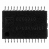
IC CLK MULT/ZD BUFFER 28-TSSOP

ICS87604AGILF

Manufacturer Part Number
ICS87604AGILF
Description
IC CLK MULT/ZD BUFFER 28-TSSOP
Manufacturer
IDT, Integrated Device Technology Inc
Series
HiPerClockS™r
Type
Clock Multiplier, Zero Delay Bufferr
Datasheet

Specifications of ICS87604AGILF

Input
LVCMOS, LVTTL
Output
LVCMOS, LVTTL
Frequency - Max
167MHz
Voltage - Supply
3.135 V ~ 3.465 V
Operating Temperature
-40°C ~ 85°C
Mounting Type
Surface Mount
Package / Case
28-TSSOP
Frequency-max
167MHz
Number Of Elements
1
Supply Current
185mA
Pll Input Freq (min)
8.33MHz
Pll Input Freq (max)
41.67MHz
Operating Supply Voltage (typ)
3.3V
Operating Temp Range
-40C to 85C
Package Type
TSSOP
Output Frequency Range
Up to 166.67MHz
Operating Supply Voltage (min)
3.135V
Operating Supply Voltage (max)
3.465V
Operating Temperature Classification
Industrial
Pin Count
28
Lead Free Status / RoHS Status
Lead free / RoHS Compliant
Other names
800-1220
800-1220-5
800-1220
87604AGILF
B
ICS87601AGI REVISION B APRIL 1, 2010
G
outputs for multiply-ing and regenerating clocks with “zero delay”.
The PLL’s VCO has an operating range of 250MHz - 500MHz,
allowing this device to be used in a variety of general purpose
clocking applications. For PCI/PCI-X applications in particular,
the VCO frequency should be set to 400MHz. This can be
accomplished by supplying 33.33MHz, 25MHz, 20MHz, or
16.66MHz on the reference clock or crystal input and by selecting
÷12, ÷16, ÷20, or ÷24, respectively as the feedback divide value.
The divider on the output bank can then be configured to generate
33.33MHz (÷12), 66.66MHz (÷6), 100MHz (÷4), or 133.33MHz
(÷3).
The ICS87604I is characterized to operate with its core
supply at 3.3V and the bank supply at 3.3V or 2.5V. The
ICS87604I is packaged in a small 6.1mm x 9.7mm TSSOP
body, making it ideal for use in space-constrained applications.
FBDIV_SEL1
FBDIV_SEL0
HiPerClockS™
XTAL_OUT
IC S
XTAL_SEL
LOCK
XTAL_IN
DIV_SEL0
DIV_SEL1
ENERAL
PLL_SEL
REF_IN
FB_IN
MR
D
OSC
The ICS87604I is a 1:4 PCI/PCI-X Clock Generator.
The ICS87604I has a selectable REF_IN or crystal
input. The REF_IN input accepts LVCMOS or LVTTL
input levels. The ICS87604I has a fully integrated PLL
along with frequency configurable clock and feedback
IAGRAM
D
ESCRIPTION
0
1
Low Voltage/Low Skew, 1:4 PCI/PCI-X
Zero Delay Clock Generator
PLL
0
1
÷12
÷16
÷20
÷24
÷12
÷3
÷4
÷6
0 0
0 1
1 0
1 1
0 0
0 1
1 0
1 1
Q0
Q1
Q2
Q3
REF_OUT
FB_OUT
1
F
Fully integrated PLL
Four LVCMOS/LVTTL outputs, 15
Selectable crystal oscillator interface or
LVCMOS/LVTTL REF_IN clock input
Maximum output frequency: 166.67MHz
Maximum crystal input frequency: 38MHz
Maximum REF_IN input frequency: 41.67MHz
Individual banks with selectable output dividers for
generating 33.333MHz, 66.66MHz, 100MHz and
133.333MHz
Separate feedback control for generating PCI / PCI-X
frequencies from a 16.66MHz or 20MHz crystal, or 25MHz
or 33.33MHz reference frequency
VCO range: 250MHz to 500MHz
Cycle-to-cycle jitter: 120ps (maximum)
Period jitter, RMS: 20ps (maximum)
Output skew: 65ps (maximum)
Static phase offset: 160ps ± 160ps
Voltage Supply Modes:
V
3.3/3.3/3.3
3.3/3.3/2.5
-40°C to 85°C ambient operating temperature
Available in both standard (RoHS 5 and lead-free (RoHS 6)
packages
EATURES
DD
/V
DDA
/V
DDO
P
REF_OUT
PLL_SEL
IN
FB_OUT
6.1mm x 9.7mm x 0.92mm
28-Lead TSSOP, 240MIL
FB_IN
GND
GND
V
V
V
A
V
DDO
DDO
Q3
Q2
Q1
Q0
DDA
DD
2010 Integrated Device Technology, Inc.
SSIGNMENT
body package
ICS87604I
G Package
Top View
1
2
3
4
5
6
7
8
9
10
11
12
13
14
typical output impedance
28
27
26
25
24
23
22
21
20
19
18
17
16
15
FBDIV_SEL1
FBDIV_SEL0
DIV_SEL1
DIV_SEL0
nc
MR
nc
GND
GND
nc
REF_IN
XTAL_OUT
XTAL_IN
XTAL_SEL
87604I

Related parts for ICS87604AGILF

ICS87604AGILF Summary of contents

Page 1

Low Voltage/Low Skew, 1:4 PCI/PCI-X Zero Delay Clock Generator G D ENERAL ESCRIPTION The ICS87604I is a 1:4 PCI/PCI-X Clock Generator The ICS87604I has a selectable REF_IN or crystal HiPerClockS™ input. The REF_IN input accepts LVCMOS or LVTTL ...

Page 2

ICS87604I ABLE IN ESCRIPTIONS ...

Page 3

ICS87604I T 3A ABLE UTPUT ONTROL IN UNCTION ...

Page 4

ICS87604I BSOLUTE AXIMUM ATINGS Supply Voltage Inputs XTAL_IN Other Inputs Outputs Package Thermal Impedance, JA Storage Temperature, T STG T 4A ABLE OWER UPPLY HARACTERISTICS S y ...

Page 5

ICS87604I ABLE RYSTAL HARACTERISTICS ...

Page 6

ICS87604I P ARAMETER 1.65V±5% 1.65V± DDO V DDA LVCMOS GND -1.65V±5% 3. UTPUT OAD EST IRCUIT V DDO DDO Qy 2 tsk( UTPUT KEW REF_IN FB_IN ...

Page 7

ICS87604I OWER UPPLY ILTERING ECHNIQUES As in any high speed analog circuitry, the power supply pins are vulnerable to random noise. To achieve optimum jitter per- formance, power supply isolation is required. The ICS87604I pro- vides ...

Page 8

ICS87604I VERDRIVING THE RYSTAL NTERFACE The XTAL_IN input can be overdriven by an LVCMOS driver or by one side of a differential driver through an AC coupling capacitor. The XTAL_OUT pin can be left floating. The amplitude ...

Page 9

ICS87604I S E CHEMATIC XAMPLE Figure 4 shows a schematic example of the ICS87604I. Series termination is shown in this schematic. Additional LVCMOS termination approaches are shown in the LVCMOS Termination Application Note. In this example parallel ...

Page 10

ICS87604I ABLE VS IR LOW ABLE FOR JA Multi-Layer PCB, JEDEC Standard Test Boards T C RANSISTOR OUNT The transistor count for ICS87604I is: 5495 P ACKAGE ...

Page 11

ICS87604I T 10 ABLE RDERING NFORMATION ...

Page 12

ICS87604I & ...

Page 13

ICS87604I www.IDT.com 6024 Silver Creek Valley Road Sales San Jose, CA 95138 800-345-7015 (inside USA) +408-284-8200 (outside USA) Fax: 408-284-2775 www.IDT.com/go/contactIDT DISCLAIMER Integrated Device Technology, Inc. (IDT) and its subsidiaries reserve the right to modify the products and/or specifications described ...

Related keywords