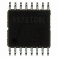
ICS557GI-08LF IDT, Integrated Device Technology Inc, ICS557GI-08LF Datasheet - Page 2

ICS557GI-08LF
Manufacturer Part Number
ICS557GI-08LF
Description
IC MUX 2:1 PCI-EXPRESS 16-TSSOP
Manufacturer
IDT, Integrated Device Technology Inc
Type
Clock Multiplexerr
Datasheet
1.ICS557G-08LF.pdf
(12 pages)
Specifications of ICS557GI-08LF
Input
HCSL, LVDS
Output
HCSL, LVDS
Frequency - Max
200MHz
Voltage - Supply
3.135 V ~ 3.465 V
Operating Temperature
-40°C ~ 85°C
Mounting Type
Surface Mount
Package / Case
16-TSSOP
Frequency-max
200MHz
Number Of Clock Inputs
2
Mode Of Operation
Differential
Output Frequency
200MHz
Output Logic Level
HCSL/LVDS
Operating Supply Voltage (min)
3.135V
Operating Supply Voltage (typ)
3.3V
Operating Supply Voltage (max)
3.465V
Package Type
TSSOP
Operating Temp Range
-40C to 85C
Operating Temperature Classification
Industrial
Signal Type
HCSL/LVDS
Mounting
Surface Mount
Pin Count
16
Lead Free Status / RoHS Status
Lead free / RoHS Compliant
Other names
557GI-08LF
800-1069
800-1069-5
800-1069
800-1069
800-1069-5
800-1069
Available stocks
Company
Part Number
Manufacturer
Quantity
Price
Company:
Part Number:
ICS557GI-08LF
Manufacturer:
IDT
Quantity:
234
Pin Assignment
Pin Descriptions
IDT® 2:1 MULTIPLEXER CHIP FOR PCI-EXPRESS
ICS557-08
2:1 MULTIPLEXER CHIP FOR PCI-EXPRESS
Pin
10
11
12
13
14
15
16
1
2
3
4
5
6
7
8
9
GND
VDD
Pin Name
IN2
IN1
IN1
IN2
PD
OE
IREF
VDD
GND
VDD
VDD
GND
GND
CLK
CLK
SEL
IN1
IN1
IN2
IN2
OE
PD
16-pin (173 mil) TSSOP
1
2
3
4
5
6
7
8
Pin Type
Output
Output
Output
Power
Power
Power
Power
Power
Power
Input
Input
Input
Input
Input
Input
Input
16
15
14
13
12
11
10
9
Connect to +3.3 V. Supply voltage for Input clocks.
HCSL/LVDS true input signal 1.
HCSL/LVDS complimentary input signal 1.
Powers down the chip and tri-states outputs when low. Internal pull-up
HCSL/LVDS true input signal 2.
HCSL/LVDS complimentary input signal 2.
Provides output or, tri-states output (High = enable outputs; Low = disable).
Internal pull-up resistor.
Connect to ground.
Precision resistor attached to this pin is connected to the internal current
Connect to +3.3 V. Supply Voltage for Output Clocks.
Connect to +3.3 V. Supply Voltage for Output Clocks.
Connect to ground.
Connect to ground.
HCSL/LVDS Complimentary output clock .
HCSL/LVDS True output clock.
SEL=1 selects IN1/IN1. SEL =0 selects IN2/ IN2. Internal pull-up resistor.
SEL
CLK
GND
GND
CLK
VDD
VDD
IREF
2
Select Table
SEL
0
1
Pin Description
Input Pair Selected
IN2/ IN2
IN1/ IN1
ICS557-08
PCIE MULTIPLEXER
REV J 121510


