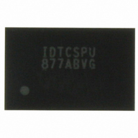
IDTCSPU877ABVG IDT, Integrated Device Technology Inc, IDTCSPU877ABVG Datasheet - Page 3

IDTCSPU877ABVG
Manufacturer Part Number
IDTCSPU877ABVG
Description
IC SDRAM CLK DVR 1:10 52-VFBGA
Manufacturer
IDT, Integrated Device Technology Inc
Type
PLL Clock Driverr
Datasheet
1.IDTCSPU877ABVG.pdf
(13 pages)
Specifications of IDTCSPU877ABVG
Input
Clock
Output
Differential
Frequency - Max
340MHz
Voltage - Supply
1.7 V ~ 1.9 V
Operating Temperature
0°C ~ 70°C
Mounting Type
Surface Mount
Package / Case
52-VFPBGA
Frequency-max
340MHz
Lead Free Status / RoHS Status
Lead free / RoHS Compliant
Other names
800-1709
CSPU877ABVG
CSPU877ABVG
Available stocks
Company
Part Number
Manufacturer
Quantity
Price
Company:
Part Number:
IDTCSPU877ABVG
Manufacturer:
TEMIC
Quantity:
277
Company:
Part Number:
IDTCSPU877ABVG
Manufacturer:
IDT, Integrated Device Technology Inc
Quantity:
10 000
Company:
Part Number:
IDTCSPU877ABVG8
Manufacturer:
IDT, Integrated Device Technology Inc
Quantity:
10 000
PIN CONFIGURATION, CONT.
RECOMMENDED OPERATING CONDITIONS
NOTE:
1. The PLL is turned off and bypassed for test purposes when AV
IDTCSPU877A
1.8V PLL DIFFERENTIAL 1:10 SDRAM CLOCK DRIVER
AGND
AV
V
V
V
GND
Symbol
parameters are guaranteed.
AV
CLK
CLK
DDQ
DDQ
DDQ
V
Y
Y
DD
DDQ
T
DD (1)
2
2
A
1
2
3
4
5
6
7
8
9
10
Supply Voltage
I/O Supply Voltage
Operating Free-Air Temperature
TOP VIEW
VFQFPN
GND
Parameter
DD
30
28
27
26
25
24
23
22
21
29
is grounded. During this test mode, V
Y
Y
V
FBIN
FBIN
FBOUT
FBOUT
OE
OS
V
7
7
DDQ
DDQ
3
ABSOLUTE MAXIMUM RATINGS
NOTES:
1. Stresses greater than those listed under ABSOLUTE MAXIMUM RATINGS may cause
2. The maximum package power dissipation is calculated using a junction temperature
3. The input and output negative-voltage ratings may be exceeded if the input and output
CAPACITANCE
NOTE:
1. Unused inputs must be held high or low to prevent them from floating.
Parameter
C
C
C
Symbol
V
V
V
I
(V
I
(V
V
I
(V
V
TSTG
IN
I
L
IK
OK
O
Δ
permanent damage to the device. This is a stress rating only and functional operation of
the device at these or any other conditions above those indicated in the operational
sections of this specification is not implied. Exposure to absolute maximum rating
conditions for extended periods may affect reliability.
of 150
clamp-current ratings are observed. This value is limited to 2.5V max.
I (3)
O (3)
DDQ
O
DDQ
I
O
O
<0)
> V
<0 or
=0 to V
, AV
or GND
°
DDQ
C and a board trace length of 750 mils.
DD
)
DDQ
DDQ
Min.
1.7
)
0
Description
Input Capacitance
V
Delta Input Capacitance
CLK, CLK, FBIN, FBIN
Load Capacitance
remains within the recommended operating conditions and no timing
I
Rating
Supply Voltage Range
Input Voltage Range
Voltage range applied to any
output in the high or low state
Input clamp current
Output Clamp Current
Continuous Output Current
Continuous Current
Storage Temperature Range
= V
DDQ
or GND
(1)
COMMERCIAL TEMPERATURE RANGE
Typ.
V
1.8
⎯
DDQ
Min.
—
2
–0.5 to V
–0.5 to V
Max.
+70
1.9
– 65 to +150
Typ.
–0.5 to +2.5
—
10
±100
Max
±50
±50
±50
DDQ
DDQ
Max.
0.25
+ 0.5
+ 0.5
(1,2)
—
3
Unit
°
V
V
C
Unit
Unit
pF
pF
pF
mA
mA
mA
mA
°C
V
V
V


