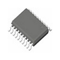
8545BGILFT IDT, Integrated Device Technology Inc, 8545BGILFT Datasheet - Page 5

8545BGILFT
Manufacturer Part Number
8545BGILFT
Description
Manufacturer
IDT, Integrated Device Technology Inc
Type
Clock Driverr
Datasheet
1.8545BGILFT.pdf
(15 pages)
Specifications of 8545BGILFT
Number Of Clock Inputs
2
Mode Of Operation
Single-Ended
Output Frequency
650MHz
Output Logic Level
LVDS
Operating Supply Voltage (min)
3.135V
Operating Supply Voltage (typ)
3.3V
Operating Supply Voltage (max)
3.465V
Package Type
TSSOP
Operating Temp Range
-40C to 85C
Operating Temperature Classification
Industrial
Signal Type
LVCMOS/LVTTL
Mounting
Surface Mount
Pin Count
20
Lead Free Status / RoHS Status
Compliant
Table 4C. LVDS DC Characteristics, V
AC Electrical Characteristics
Table 5. AC Characteristics, V
All parameters measured at ƒ ≤ 650MHz unless noted otherwise.
NOTE 1: Measured from V
NOTE 2: Defined as skew between outputs at the same supply voltage and with equal load conditions.
Measured at V
NOTE 3: Defined as skew between outputs on different devices operating at the same supply voltages and with equal load conditions.
Using the same type of inputs on each device, the outputs are measured at the differential cross points.
NOTE 4: This parameter is defined in accordance with JEDEC Standard 65.
IDT™ / ICS™ LVDS FANOUT BUFFER
Symbol
V
∆V
V
∆V
I
I
I
I
V
V
Parameter Symbol
f
t
tjit
tsk(o)
tsk(pp)
t
odc
Oz
OFF
OSD
OS
MAX
PD
R
ICS8545I
LOW SKEW, 1-TO-4, LVCMOS/LVTTL-TO-LVDS FANOUT BUFFER
OD
OS
OH
OL
/ t
OD
OS
F
Parameter
Differential Output Voltage
V
Offset Voltage
V
High Impedance Leakage
Power Off Leakage
Differential Output Short Circuit Current
Output Short Circuit Current
Output Voltage High
Output Voltage Low
OD
OS
Output Frequency
Propagation Delay; NOTE 1
Buffer Additive Phase Jitter, RMS;
refer to Additive Phase Jitter Section
Output Skew; NOTE 2, 4
Part-to-Part Skew; NOTE 3, 4
Output Rise/Fall Time
Output Duty Cycle
DD
/2 of the input to the differential output crossing point.
Magnitude Change
Magnitude Change
DD
/2 of the input to the differential output crossing point.
DD
= 3.3V ± 5%, T
DD
= 3.3V ± 5%, T
A
156.25MHz, Integration Range:
= -40°C to 85°C
Test Conditions
20% to 80% @ 50MHz
Test Conditions
12kHz – 20MHz
A
ƒ ≤ 266MHz
ƒ > 266MHz
ƒ ≤ 650MHz
= -40°C to 85°C
5
Minimum
1.125
200
-10
-20
0.9
Minimum
200
1.4
45
40
Typical
1.25
1.34
1.06
ICS8545BGI REV. B MARCH 02, 2009
-3.5
-3.5
280
±1
±1
5
Typical
0.13
400
Maximum
1.375
Maximum
360
+10
+20
1.6
40
25
-5
-5
650
500
700
3.6
40
55
60
Units
mV
mV
mV
mA
mA
Units
µA
µA
MHz
V
V
V
ns
ps
ps
ps
ps
%
%


