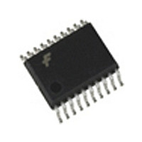
FM3570MT20 Fairchild Semiconductor, FM3570MT20 Datasheet - Page 3

FM3570MT20
Manufacturer Part Number
FM3570MT20
Description
Manufacturer
Fairchild Semiconductor
Datasheet
1.FM3570MT20.pdf
(8 pages)
Specifications of FM3570MT20
Operating Temperature (min)
0C
Operating Temperature (max)
70C
Operating Temperature Classification
Commercial
Mounting
Surface Mount
Pin Count
20
Package Type
TSSOP
Lead Free Status / RoHS Status
Compliant
Available stocks
Company
Part Number
Manufacturer
Quantity
Price
Part Number:
FM3570MT20
Manufacturer:
F
Quantity:
20 000
Company:
Part Number:
FM3570MT20X
Manufacturer:
FSC
Quantity:
6 942
Company:
Part Number:
FM3570MT20X
Manufacturer:
TOS
Quantity:
834
Part Number:
FM3570MT20X
Manufacturer:
FAIRCHILD/仙童
Quantity:
20 000
FM3570 Rev. A
The FM3570 block diagram is shown in Figure 1. The device has
two primary functional modes of operationi and an additional
mode for programming the device.
Operational Modes
During standard operation, the device will either pass an address
to the Y-Port from the I-Port or from an internally programmed
value.
The I-port values are generated from the motherboard of the
system and may be hardwired or driven by another device. Pull-
up resistors are provided on the device to accommodate this
device being driven by open-drain output drivers. The voltage
level to which the I-port is pulled up to is determined by the voltage
on the EPV pin. The device expects standard CMOS input signals.
The the non-multiplexed output is always at CMOS levels. The
OVRD (override) input, when set to 0, will cause all the outputs to
be set to 0. The WP signal, if set to logic 1, will prevent data from
being written to the non-volatile register.
The MUXSEL input, when set to logic 0, will select the data from
the non-volatile register to drive on the Y0-4 outputs. if set to logic
1, the data from the inputs are selected instead. the non_mux_out
latch is transparent when the MUXSEL signal is at logic 0, and will
latch when the MUXSEL is in a logic 1 state.
The output port is an open-drain output to allow for easy connec-
tion to devices running at different voltage levels. The port is
always active and either passes the value on the I-Port or the value
in the Serial output port (SOPR). Changing the Mux Path is
accomplished by writing to b7 of the Serial Input Port Register.
SOPR-b7 defaults to a value of zero at power up and the default
path is from the I-port though to the output port. The multiplexer
only updates when an IIC stop condition is observed.
The FM3570 has 3 registers in total. These registers are made up
of a combination of read-only, write-only and read/write bits. The
two registers are listed below.
Serial Output Port Register A(SOPRA) Address: 00H - A read/
write register that contains the new value to be written to output
Port-Y and the multiplexer select bit.
Serial Output Port Register B(SOPRB) Address: 01H - A read/
write register that contains the new value to be written to output
Port-Y and the multiplexer select bit.
Parallel Input Port Register (PIPR) Address: 02H - A read-only
register that is loaded with the 5-bit value of the I-Port.
(Address 000b and 001b)
b7-b6 - Multiplexer Select Bits (MXSB, MXSA)
00 - Multiplexer passes the SOPR(A).
01 - Multiplexer passer the SOPR(B).
10 - Multiplexer defaults to passing the I-Port Value.
b5, b3-b0 - Data Field. New value to be output through the
multiplexer.
NMO - Non-multiplexed output from internal non-volatile bit.
(Address 002b)
b7-b5 - Address field. Value is always 000
b4-b0 - Data Field. Value is equal to the value on the I-Port.
The external Port Register captures the value on the I-Port. Data
is latched into this register on the first clock after a start condition
is seen. This insures that a valid value will always be in this register
if it is read. This register is a-read only register with respect to the
IIC port.
b7
b7
0
0
b6
b6
0
0
b5
b5
I5
0
NMO
b4
b4
I4
b3
b3
I3
I3
b2
b2
I2
I2
www.fairchildsemi.com
www.fairchildsemi.com
b1
B1
I1
I1
b0
b0
I0
I0


