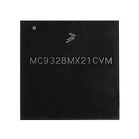
MC9328MX21CVM Freescale, MC9328MX21CVM Datasheet - Page 54

MC9328MX21CVM
Manufacturer Part Number
MC9328MX21CVM
Description
Manufacturer
Freescale
Datasheet
1.MC9328MX21CVM.pdf
(100 pages)
Specifications of MC9328MX21CVM
Operating Temperature (min)
-40C
Operating Temperature (max)
85C
Operating Temperature Classification
Industrial
Mounting
Surface Mount
Lead Free Status / RoHS Status
Compliant
Available stocks
Company
Part Number
Manufacturer
Quantity
Price
Company:
Part Number:
MC9328MX21CVM
Manufacturer:
Freescale Semiconductor
Quantity:
10 000
Company:
Part Number:
MC9328MX21CVMR2
Manufacturer:
Freescale Semiconductor
Quantity:
10 000
Specifications
1. All the timings for the SSI are given for a non-inverted serial clock polarity (TSCKP/RSCKP = 0) and a non- inverted frame sync
54
Ref
No.
Ref
No.
11a
11b
(TFSI/RFSI = 0). If the polarity of the clock and/or the frame sync have been inverted, all the timing remains valid by inverting
the clock signal STCK/SRCK and/or the frame sync STFS/SRFS shown in the tables and in the figures.
31
32
33
34
10
12
13
14
15
16
17
18
19
1
2
3
4
5
6
7
8
9
SRXD setup before (Tx) CK falling
SRXD hold after (Tx) CK falling
SRXD setup before (Tx) CK falling
SRXD hold after (Tx) CK falling
(Tx/Rx) CK clock period
(Tx) CK high to FS (bl) high
(Rx) CK high to FS (bl) high
(Tx) CK high to FS (bl) low
(Rx) CK high to FS (bl) low
(Tx) CK high to FS (wl) high
(Rx) CK high to FS (wl) high
(Tx) CK high to FS (wl) low
(Rx) CK high to FS (wl) low
(Tx) CK high to STXD valid from high impedance
(Tx) CK high to STXD high
(Tx) CK high to STXD low
(Tx) CK high to STXD high impedance
SRXD setup time before (Rx) CK low
SRXD hold time after (Rx) CK low
(Tx/Rx) CK clock period
(Tx/Rx) CK clock high period
(Tx/Rx) CK clock low period
(Tx) CK high to FS (bl) high
(Rx) CK high to FS (bl) high
Table 34. SSI to SAP Ports Timing Parameters (Continued)
Parameter
Parameter
1
1
9
9
Synchronous External Clock Operation (SAP Ports)
Table 35. SSI to SSI1 Ports Timing Parameters
Synchronous Internal Clock Operation (SAP Ports)
MC9328MX21 Technical Data, Rev. 3.4
Internal Clock Operation
External Clock Operation (SSI1 Ports)
Minimum
Minimum
20.41
36.36
36.36
10.22
10.79
23.00
-0.68
-0.96
-0.68
-0.96
-0.68
-0.96
-0.68
-0.96
-1.68
-1.68
-1.68
-1.58
1.20
0.91
0.91
0
0
0
1
1.8 V ± 0.1 V
1.8 V ± 0.1 V
(SSI1 Ports)
Maximum
Maximum
17.63
19.67
-0.15
-0.27
-0.15
-0.27
-0.15
-0.27
-0.15
-0.27
-0.36
-0.36
-0.36
-0.31
–
–
–
–
–
–
–
–
–
–
Minimum
Minimum
90.91
20.41
90.91
36.36
36.36
21.41
-0.68
-0.96
-0.68
-0.96
-0.68
-0.96
-0.68
-0.96
-1.68
-1.68
-1.68
-1.58
8.82
9.39
0.88
0
0
0
3.0 V ± 0.3 V
3.0 V ± 0.3 V
Freescale Semiconductor
Maximum
Maximum
16.24
18.28
-0.15
-0.27
-0.15
-0.27
-0.15
-0.27
-0.15
-0.27
-0.36
-0.36
-0.36
-0.31
–
–
–
–
–
–
–
–
–
–
Unit
Unit
ns
ns
ns
ns
ns
ns
ns
ns
ns
ns
ns
ns
ns
ns
ns
ns
ns
ns
ns
ns
ns
ns
ns
ns


