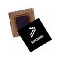
MPC8270CVVUPEA Freescale, MPC8270CVVUPEA Datasheet - Page 19

MPC8270CVVUPEA
Manufacturer Part Number
MPC8270CVVUPEA
Description
Manufacturer
Freescale
Datasheet
1.MPC8270CVVUPEA.pdf
(80 pages)
Specifications of MPC8270CVVUPEA
Family Name
MPC82XX
Device Core
PowerQUICC II
Device Core Size
32b
Frequency (max)
450MHz
Instruction Set Architecture
RISC
Operating Supply Voltage (max)
1.6V
Operating Supply Voltage (min)
1.45V
Operating Temp Range
-40C to 105C
Operating Temperature Classification
Industrial
Mounting
Surface Mount
Pin Count
480
Package Type
TBGA
Lead Free Status / RoHS Status
Compliant
Available stocks
Company
Part Number
Manufacturer
Quantity
Price
Company:
Part Number:
MPC8270CVVUPEA
Manufacturer:
Freescale Semiconductor
Quantity:
135
Company:
Part Number:
MPC8270CVVUPEA
Manufacturer:
FREE
Quantity:
4
Company:
Part Number:
MPC8270CVVUPEA
Manufacturer:
Freescale Semiconductor
Quantity:
10 000
Part Number:
MPC8270CVVUPEA
Manufacturer:
NXP/恩智浦
Quantity:
20 000
6.2 SIU AC Characteristics
Note the following points about the SIU AC characteristics:
Table 11
Table 12
Freescale Semiconductor
1
Setup
Spec Number
sp13a
sp14a
Spec Number
sp33a
sp12
sp13
sp14
sp15
sp31
sp32
sp11
Max
measured at the pin.
Input specifications are measured from the 50% level of the signal to the 50% level of the rising edge of CLKIN. Timings are
•
•
•
•
CLKIN jitter and duty cycle. The CLKIN input to the MPC8280 should not exceed +/– 150 psec of jitter
(peak-to-peak). This represents total input jitter—the combination of short term (cycle-to-cycle) and long
term (cumulative). The duty cycle of CLKIN should not exceed the ratio of 40:60. The rise/file time of
CLKIN should adhere to the typical SDRAM device AC clock requirement of 1 V/ns to meet SDRAM AC
specs.
Spread spectrum clocking. Is allowed with 1% input frequency down-spread at maximum 60 KHz
modulation rate regardless of input frequency.
PCI AC timing. The MPC8280 meets the timing requirements of PCI Specification Revision 2.2. Refer to
Sections 7.2 and 7.3 and “Note: Tval (Output Hold)” to determine if a specific clock configuration is
compliant.
Activating data pipelining (setting BRx[DR] in the memory controller) improves the AC timing.
lists SIU input characteristics.
lists SIU output characteristics.
Hold
sp10 AACK/TA/TS/DBG/BG/BR/ARTRY/
sp10 Data bus in normal mode
sp10 Data bus in ECC and PARITY modes
sp10 Pipeline mode—Data bus (with or without
sp10 DP pins
sp10 Pipeline mode—DP pins
sp10 All other pins
sp30 PSDVAL/TEA/TA
sp30 ADD/ADD_atr./BADDR/CI/GBL/WT
sp30 Data bus
Min
TEA
ECC/PARITY)
MPC8280 PowerQUICC™ II Family Hardware Specifications, Rev. 1.8
2
Characteristic
Characteristic
Table 12. AC Characteristics for SIU Outputs
Table 11. AC Characteristics for SIU Inputs
66 MHz
66 MHz
—
6.5
6
5
7
5
7
5
7
8
Maximum Delay
83 MHz
83 MHz
Setup
6.5
6.5
5
4
5
4
5
4
4
6
100 MHz
100 MHz
3.5
3.5
3.5
2.5
3.5
2.5
3.5
5.5
5.5
5.5
Value (ns)
Value (ns)
1
1
66 MHz
66 MHz
AC Electrical Characteristics
0.5
0.5
0.5
0.5
0.5
0.5
0.7
—
1
1
Minimum Delay
83 MHz
83 MHz
Hold
0.5
0.5
0.5
0.5
0.5
0.5
0.5
0.7
1
1
100 MHz
100 MHz
0.5
0.5
0.5
0.5
0.5
0.5
0.5
0.7
1
1
19


