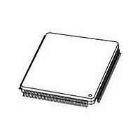
LH79525N0Q100A1 Sharp Electronics, LH79525N0Q100A1 Datasheet - Page 14

LH79525N0Q100A1
Manufacturer Part Number
LH79525N0Q100A1
Description
Manufacturer
Sharp Electronics
Datasheet
1.LH79525N0Q100A1.pdf
(64 pages)
Specifications of LH79525N0Q100A1
Operating Temperature (min)
-40C
Operating Temperature (max)
85C
Applications
Embedded Control
Processing Unit
Microcontroller
Operating Supply Voltage (min)
1.7/3V
Operating Supply Voltage (typ)
1.8/3.3V
Operating Supply Voltage (max)
1.9/3.6V
Package Type
LQFP
Screening Level
Industrial
Pin Count
176
Mounting
Surface Mount
Rad Hardened
No
Lead Free Status / RoHS Status
Compliant
Available stocks
Company
Part Number
Manufacturer
Quantity
Price
Company:
Part Number:
LH79525N0Q100A1
Manufacturer:
FREESCALE
Quantity:
101
Company:
Part Number:
LH79525N0Q100A1,55
Manufacturer:
NXP Semiconductors
Quantity:
10 000
LH79524/LH79525
14
PIN NO.
20
19
15
12
13
16
18
25
36
35
34
32
31
30
29
28
44
43
42
41
40
39
38
37
60
59
58
56
55
54
AN3/LR/Y–/PJ0
AN4/WIPER/PJ1
AN5/PJ5/INT5
AN6/PJ7/INT7
AN7/PJ6/INT6
AN8/PJ4
AN9/PJ2
CTCLK/INT4/
BATCNTL
PA0/UARTRX2/
UARTIRRX2/INT2
PA1/UARTTX2/
UARTIRRX2/INT3
PA2/CTCAP0A/
CTCMP0A
PA3/CTCAP0B/
CTCMP0B
PA4/CTCAP1A/
CTCMP1A
PA5/CTCAP1B/
CTCMP1B
PA6/CTCAP2A/
CTCMP2A/SDA
PA7/CTCAP2B/
CTCMP2B/SLC
PB0/nDACK/
nUARTCTS0
PB1/DREQ/
nUARTRTS0
PB2/SSPFRM/
I2SWS
PB3/SSPCLK/
I2SCLK
PB4/SSPRX/
I2SRXD/UARTRX1/
UARTIRRX1
PB5/SSPTX/
I2STXD/UARTTX1/
UARTIRTX1
PB6/INT0/
UARTRX0/
UARTIRRX0
PB7/INT1/
UARTTX0/
UARTIRTX0
PC0/A16
PC1/A17
PC2/A18
PC3/A19
PC4/A20
PC5/A21
SIGNAL NAME
TYPE
I/O
I/O
I/O
I/O
I/O
I/O
I/O
I/O
I/O
I/O
I/O
I/O
I/O
I/O
I/O
I/O
I/O
I/O
I/O
I/O
I/O
I/O
I/O
I
I
I
I
I
I
I
Table 5. LH79525 Pin Descriptions (Cont’d)
ADC Input 3, 4 wire touch screen Upper Right, 5 wire touch screen Y–; multiplexed
with GPIO Port J0 (input only)
ADC Input 4, 5 wire touch screen Wiper input; multiplexed with Port J1 (input only)
ADC Input 5; multiplexed with GPIO Port J5 (input only) and External Interrupt 5
ADC Input 6; multiplexed with GPIO Port J7 (input only) and External Interrupt 7
ADC Input 7; multiplexed with GPIO Port J6 (input only) and External Interrupt 6
ADC Input 8; multiplexed with GPIO Port J4 (input only)
ADC Input 9; multiplexed with GPIO Port J2 (input only)
Timer[2:0] External Clock input; multiplexed with Battery Control and Interrupt 4
General Purpose I/O Signal — Port A0; multiplexed with UART2 Received Serial
Data Input, UART2 Infrared Received Serial Data In, and External Interrupt 2
General Purpose I/O Signal — Port A1; multiplexed with UART2 Transmitted
Serial Data Output, UART2 Serial Transmit Data Out, and External Interrupt 3
General Purpose I/O Signal — Port A2; multiplexed with Counter/Timer 0 Capture A
input and Counter/Timer 0 Compare A output
General Purpose I/O Signal — Port A3; multiplexed with Counter/Timer 0 Capture B
input and Counter/Timer 0 Compare B output
General Purpose I/O Signal — Port A4; multiplexed with Counter/Timer 1 Capture A
input and Counter/Timer 1 Compare A output
General Purpose I/O Signal — Port A5; multiplexed with Counter/Timer 1 Capture B
input and Counter/Timer 1 Compare B output
General Purpose I/O Signal — Port A6; multiplexed with Counter/Timer 2 Capture A
input, Counter/Timer 2 Compare A output, and I
General Purpose I/O Signal — Port A7; multiplexed with Counter/Timer 2 Capture B
input, Counter/Timer 2 Compare B output, and I
General Purpose I/O Signal — Port B0; multiplexed with DMA Acknowledge and
UART0 CTS
General Purpose I/O Signal — Port B1; multiplexed with DMA Request and
UART0 RTS
General Purpose I/O Signal — Port B2; multiplexed with SSP Serial Frame Output
and I
General Purpose I/O Signal — Port B3; multiplexed with SSP Clock and I
General Purpose I/O Signal — Port B4; multiplexed with SSP Data In, I
UART1 Serial Data In, and UART1 Infrared Data In
General Purpose I/O Signal — Port B5; multiplexed with SSP Data Out, I
UART1 Data Out, and UART1 IR Data Out
General Purpose I/O Signal — Port B6; multiplexed with UART0 Infrared Received
Serial Data Input, UART0 Received Serial Data In, and External Interrupt 0
General Purpose I/O Signal — Port B7; multiplexed with UART0 Infrared Transmitted
Serial Data Output, UART0 Serial Transmit Data Out, and External Interrupt 1
General Purpose I/O Signal — Port C0; multiplexed with Address A16
General Purpose I/O Signal — Port C1; multiplexed with Address A17
General Purpose I/O Signal — Port C2; multiplexed with Address A18
General Purpose I/O Signal — Port C3; multiplexed with Address A19
General Purpose I/O Signal — Port C4; multiplexed with Address A20
General Purpose I/O Signal — Port C5; multiplexed with Address A21
2
S Frame Output
Rev. 02 — 17 March 2009
NXP Semiconductors
DESCRIPTION
2
2
C Bus Data (open drain)
C Bus Clock (open drain)
Product data sheet
System-on-Chip
2
2
S Data In,
S Data Out,
2
S Clock


