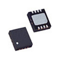
LTC2908CDDB-A1#PBF Linear Technology, LTC2908CDDB-A1#PBF Datasheet - Page 8

LTC2908CDDB-A1#PBF
Manufacturer Part Number
LTC2908CDDB-A1#PBF
Description
Manufacturer
Linear Technology
Datasheet
1.LTC2908CDDB-A1PBF.pdf
(16 pages)
Specifications of LTC2908CDDB-A1#PBF
Voltage Supervisor Type
Voltage Monitor
Number Of Voltage Supervisors
6
Operating Supply Voltage (min)
0.5V
Operating Supply Voltage (max)
6V
Package Type
DFN
Operating Temperature Classification
Commercial
Operating Temp Range
0C to 70C
Pin Count
8
Mounting
Surface Mount
Lead Free Status / RoHS Status
Compliant
Available stocks
Company
Part Number
Manufacturer
Quantity
Price
LTC2908
PIN FUNCTIONS
V1 (Pin 1/Pin 4): Voltage Input 1. V1 is the internal V
The operating voltage on this pin shall not exceed 6V.
When in normal operation, this pin draws approximately
22μA. Bypass this pin to ground with a 0.1μF (or greater)
capacitor.
V
for recommended ADJ resistors values.
RST (Pin 3/Pin 4): Reset Logic Output. Pulls low when
any voltage input is below the reset threshold and is held
low for 200ms after all voltage inputs are above threshold.
This pin has a weak pull-up to Vcc and may be pulled above
Vcc using an external pull-up.
BLOCK DIAGRAMS
8
ADJ5
(Pin 2/Pin 3): Adjustable Voltage Input 5. See Table 1
V1
V2
V3
V4
V
V
GND
ADJ1
ADJ2
DETECT
POWER
(TS8 Package/DDB8 Package) LTC2908-C1
V
CC
–
–
–
–
–
–
+
+
+
+
+
+
C1
C2
C3
C4
C5
C6
REFERENCE
BANDGAP
CC
.
GND (Pin 4/Pin 1): Device Ground.
V
See Table 1 for recommended ADJ resistors values.
V
See Table 1 for recommended ADJ resistors values.
V
See Table 1 for recommended ADJ resistors values.
V
See Table 1 for recommended ADJ resistors values.
Exposed Pad (Pin 9, DDB8 Only): Exposed Pad may be
left open or connected to device ground.
ADJ4
ADJ3
ADJ2
ADJ1
(Pin 5/Pin 8): Adjustable Voltage Input 4.
(Pin 6/Pin 7): Adjustable Voltage Input 3.
(Pin 7/Pin 6): Adjustable Voltage Input 2.
(Pin 8/Pin 5): Adjustable Voltage Input 1.
RESET PULSE
GENERATOR
200ms
LTC2908-A1/LTC2908-B1
6μA
V
CC
RST
2908 BD
2908fc


