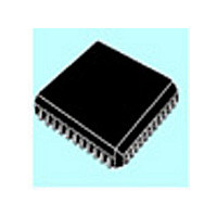
M27C1024-10K7 STMicroelectronics, M27C1024-10K7 Datasheet - Page 3

M27C1024-10K7
Manufacturer Part Number
M27C1024-10K7
Description
Manufacturer
STMicroelectronics
Datasheet
1.M27C1024-10K7.pdf
(16 pages)
Specifications of M27C1024-10K7
Lead Free Status / RoHS Status
Supplier Unconfirmed
Table 2. Absolute Maximum Ratings
Note: 1. Except for the rating ”Operating Temperature Range”, stresses above those listed in the Table ”Absolute Maximum Ratings” may
Table 3. Operating Modes
Note: X = V
Table 4. Electronic Signature
Note: Outputs Q15-Q8 are set to ’0’.
Read
Output Disable
Program
Verify
Program Inhibit
Standby
Electronic Signature
Manufacturer’s Code
Device Code
Symbol
V
V
T
T
2. Minimum DC voltage on Input or Output is –0.5V with possible undershoot to –2.0V for a period less than 20ns. Maximum DC
3. Depends on range.
V
V
A9
IO
BIAS
T
STG
Identifier
CC
PP
A
cause permanent damage to the device. These are stress ratings only and operation of the device at these or any other conditions
above those indicated in the Operating sections of this specification is not implied. Exposure to Absolute Maximum Rating condi-
tions for extended periods may affect device reliability. Refer also to the STMicroelectronics SURE Program and other relevant qual-
ity documents.
voltage on Output is V
(2)
(2)
IH
or V
Mode
IL
Ambient Operating Temperature
Temperature Under Bias
Storage Temperature
Input or Output Voltage (except A9)
Supply Voltage
A9 Voltage
Program Supply Voltage
, V
ID
= 12V
CC
V
A0
V
IH
IL
0.5V.
+0.5V with possible overshoot to V
Q7
0
1
V
V
V
V
V
V
V
E
IL
IL
IL
IL
IH
IH
IL
Parameter
(1)
Q6
0
0
(3)
V
V
V
V
G
X
X
X
IH
IL
IL
IL
Q5
1
0
CC
+2V for a period less than 20ns.
Q4
V
0
0
IL
V
V
V
Pulse
P
X
X
X
IH
IH
IH
Q3
0
1
V
Q2
A9
X
X
X
X
X
X
0
1
ID
–40 to 125
–50 to 125
–65 to 150
Q1
–2 to 13.5
0
0
–2 to 14
V
V
V
–2 to 7
–2 to 7
Value
CC
CC
CC
V
V
V
V
V
or V
or V
or V
CC
PP
PP
PP
PP
Q0
0
0
SS
SS
SS
M27C1024
Data Output
Data Output
Data Input
Hex Data
Q15-Q0
Codes
Hi-Z
Hi-Z
Hi-Z
8Ch
20h
Unit
V
V
V
V
C
C
C
3/16


