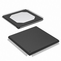
XC3S250E-4TQG144I Xilinx Inc, XC3S250E-4TQG144I Datasheet - Page 177

XC3S250E-4TQG144I
Manufacturer Part Number
XC3S250E-4TQG144I
Description
FPGA Spartan®-3E Family 250K Gates 5508 Cells 572MHz 90nm (CMOS) Technology 1.2V 144-Pin TQFP
Manufacturer
Xilinx Inc
Series
Spartan™-3Er
Datasheet
1.XC3S100E-4VQG100C.pdf
(233 pages)
Specifications of XC3S250E-4TQG144I
Package
144TQFP
Family Name
Spartan®-3E
Device Logic Cells
5508
Device Logic Units
612
Device System Gates
250000
Number Of Registers
4896
Maximum Internal Frequency
572 MHz
Typical Operating Supply Voltage
1.2 V
Maximum Number Of User I/os
108
Ram Bits
221184
Number Of Logic Elements/cells
5508
Number Of Labs/clbs
612
Total Ram Bits
221184
Number Of I /o
108
Number Of Gates
250000
Voltage - Supply
1.14 V ~ 1.26 V
Mounting Type
Surface Mount
Operating Temperature
-40°C ~ 100°C
Package / Case
144-LQFP
Lead Free Status / RoHS Status
Lead free / RoHS Compliant
For Use With
813-1009 - MODULE USB-TO-FPGA TOOL W/MANUAL
Lead Free Status / RoHS Status
Lead free / RoHS Compliant
Available stocks
Company
Part Number
Manufacturer
Quantity
Price
Company:
Part Number:
XC3S250E-4TQG144I
Manufacturer:
XILINX
Quantity:
1 670
Company:
Part Number:
XC3S250E-4TQG144I
Manufacturer:
XILINX
Quantity:
284
Company:
Part Number:
XC3S250E-4TQG144I
Manufacturer:
Xilinx Inc
Quantity:
10 000
Part Number:
XC3S250E-4TQG144I
Manufacturer:
XILINX/赛灵思
Quantity:
20 000
User I/Os by Bank
Table 134
tributed on the XC3S100E FPGA packaged in the CP132
package.
Table 134: User I/Os Per Bank for the XC3S100E in the CP132 Package
Table 135: User I/Os Per Bank for the XC3S250E and XC3S500E in the CP132 Package
DS312-4 (v3.8) August 26, 2009
Product Specification
Notes:
1.
2.
Notes:
1.
2.
Top
Right
Bottom
Left
TOTAL
Top
Right
Bottom
Left
TOTAL
Package
Package
Some VREF and CLK pins are on INPUT pins.
The eight global clock pins in this bank have optional functionality during configuration and are counted in the DUAL column.
Some VREF and CLK pins are on INPUT pins.
The eight global clock pins in this bank have optional functionality during configuration and are counted in the DUAL column.
Edge
Edge
Table 135
shows how the 83 available user-I/O pins are dis-
R
I/O Bank
I/O Bank
indicates how the 92 available user-I/O
0
1
2
3
0
1
2
3
Maximum
Maximum
I/O
I/O
18
23
22
20
83
22
23
26
21
92
I/O
I/O
10
16
11
11
22
6
0
0
0
0
www.xilinx.com
pins are distributed on the XC3S250E and the XC3S500E
FPGAs in the CP132 package.
INPUT
INPUT
2
0
0
0
2
0
0
0
0
0
All Possible I/O Pins by Type
All Possible I/O Pins by Type
DUAL
DUAL
21
20
42
21
24
46
1
0
1
0
VREF
VREF
1
2
2
2
7
2
2
2
2
8
Pinout Descriptions
(1)
(1)
CLK
CLK
0
0
0
0
16
16
8
8
8
8
(2)
(2)
(2)
(2)
(1)
(1)
177


