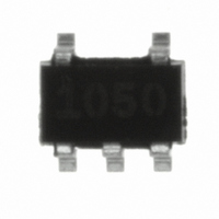
ZXCT1050E5TA Diodes Zetex, ZXCT1050E5TA Datasheet - Page 7

ZXCT1050E5TA
Manufacturer Part Number
ZXCT1050E5TA
Description
Precision Wide Input Range Current Monitor 5-Pin SOT-23 T/R
Manufacturer
Diodes Zetex
Datasheet
1.ZXCT1050E5TA.pdf
(10 pages)
Specifications of ZXCT1050E5TA
Package
5SOT-23
Operating Temperature
-40 to 125 °C
Function
Current Monitor
Sensing Method
High/Low-Side
Accuracy
±3%
Voltage - Input
2.7 ~ 20 V
Mounting Type
Surface Mount
Package / Case
SOT-23-5, SC-74A, SOT-25
Lead Free Status / RoHS Status
Lead free / RoHS Compliant
Current - Output
-
Lead Free Status / RoHS Status
Lead free / RoHS Compliant
Other names
ZXCT1050E5TR
Applications information
The ZXCT1050 is a current output version of the ZXCT1051 and as such uses a separate power
supply pin. All biasing for the internal amplifiers comes from its separate V
powered’, unlike the ZXCT1021.
This means that at very small sense voltages the ZXCT1050 draws very little current (<1 A) from
the lines being sensed.
The separate V
where the ZXCT1021 would switch off. This feature enables the ZXCT1050 to be used to sense the
currents flowing through lines that have been shorted to ground.
Basic operation
Load current, I
sense inputs of the ZXCT1050.
The internal amplifier forces V
causing a current to flow through transistor Q1 and out of the output pin, OUT. This current is then
converted to a voltage by a resistor, R
The overall gain of the ZXCT1050 is determined by the following expression:
A ratio of 1:2 between R
RG (see electrical characteristics for output current-voltage characteristics).
The ZXCT1050 has both R
required gain can be achieved at the required output impedance.
For low power applications both R
R
The maximum recommended value for R
RSH is 10k . Large values of R
of R
The maximum differential input voltage, V
500mV will not damage it. This can be increased further by the inclusion of a resistor, R
between the SENSE+ pin and the rail being sensed, V
For best performance R
minimizing any series resistance with R
Issue 1 - June 2007
© Zetex Semiconductors plc 2007
G
and R
G
can created load errors and reduce bandwidths.
GAIN
SH
can be decreased.
=
L
CC
, from V
20
pin enables the ZXCT1050 to be operated at sense line voltages down to 0V,
GND
×
V
RAIL
--------- -
R
R
SENSE
SH
RAIL
SH
SENSE+ (4)
G
V
and R
G
(1)
CC
and R
is drawn through R
should be connected as close to the SENSE+ and SENSE- pins thus
SH
SENSE
GND (2)
G
start increasing the effective input offset error, while large values
G
creates the fixed gain of 10 with an output impedance equal to
SH
and R
R
across external resistance R
G
external. This allows R
SENSE
, between OUT and GND.
SENSE
ZXCT1050
SH
G
SENSE
Q1
(5) SENSE-
can be increased whereas for driving low impedance
is 40k
.
7
, is 150mV (I
R
SENSE
SH
and the maximum recommended value for
RAIL
Out
(3)
developing a voltage V
.
R
L
G
G
* R
and R
SENSE
SH
(internal on the ZXCT1051)
SH
Load
); however voltages up to
I
to be varied so that the
L
CC
input and is not ‘line
ZXCT1050
SENSE
www.zetex.com
across the
LIM
,


