PIC12LF1840-E/MF Microchip Technology, PIC12LF1840-E/MF Datasheet - Page 183
PIC12LF1840-E/MF
Manufacturer Part Number
PIC12LF1840-E/MF
Description
7 KB Flash, 256 Bytes RAM, 32 MHz Int. Osc, 6 I/0, Enhanced Mid Range Core, Nano
Manufacturer
Microchip Technology
Series
PIC® XLP™ 12Fr
Datasheet
1.PIC12F1840-EMF.pdf
(382 pages)
Specifications of PIC12LF1840-E/MF
Processor Series
PIC12F
Core
PIC
Program Memory Type
Flash
Program Memory Size
7 KB
Data Ram Size
256 B
Interface Type
MI2C, SPI, EUSART
Number Of Timers
3
Operating Supply Voltage
1.8 V to 5.5 V
Maximum Operating Temperature
+ 125 C
Mounting Style
SMD/SMT
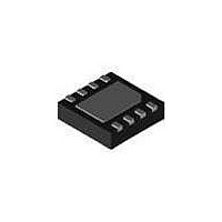
Package / Case
DFN-8
Development Tools By Supplier
MPLAB IDE Software
Minimum Operating Temperature
- 40 C
Core Processor
RISC
Core Size
8-Bit
Speed
32MHz
Connectivity
I²C, LIN, SPI, UART/USART
Peripherals
Brown-out Detect/Reset, POR, PWM, WDT
Number Of I /o
5
Eeprom Size
256 x 8
Ram Size
256 x 8
Voltage - Supply (vcc/vdd)
1.8 V ~ 3.6 V
Data Converters
A/D 4x10b
Oscillator Type
Internal
Operating Temperature
-40°C ~ 125°C
Lead Free Status / Rohs Status
Details
Available stocks
Company
Part Number
Manufacturer
Quantity
Price
Company:

Part Number:
PIC12LF1840-E/MF
Manufacturer:
MICROCHIP
Quantity:
12 000


23.5
The signal provided from any selected input source for
the carrier high and carrier low signals can be inverted.
Inverting the signal for the carrier high source is
enabled by setting the MDCHPOL bit of the MDCARH
register. Inverting the signal for the carrier low source is
enabled by setting the MDCLPOL bit of the MDCARL
register.
23.6
Some peripherals assert control over their correspond-
ing output pin when they are enabled. For example,
when the CCP1 module is enabled, the output of CCP1
is connected to the CCP1 pin.
This default connection to a pin can be disabled by set-
ting the MDCHODIS bit in the MDCARH register for the
carrier high source and the MDCLODIS bit in the
MDCARL register for the carrier low source.
23.7
The MDBIT of the MDCON register can be selected as
the source for the modulator signal. This gives the user
the ability to program the value used for modulation.
23.8
The modulator source default connection to a pin can
be disabled by setting the MDMSODIS bit in the
MDSRC register.
23.9
The modulated output signal provided on the MDOUT
pin can also be inverted. Inverting the modulated out-
put signal is enabled by setting the MDOPOL bit of the
MDCON register.
23.10 Slew Rate Control
The slew rate limitation on the output port pin can be
disabled. The slew rate limitation can be removed by
clearing the MDSLR bit in the MDCON register.
2011 Microchip Technology Inc.
Carrier Source Polarity Select
Carrier Source Pin Disable
Programmable Modulator Data
Modulator Source Pin Disable
Modulated Output Polarity
Preliminary
23.11 Operation in Sleep Mode
The Data Signal Modulator (DSM) module is not
affected by Sleep mode. The DSM can still operate
during Sleep, if the carrier and modulator input sources
are also still operable during Sleep.
23.12 Effects of a Reset
Upon any device Reset, the DSM module is disabled.
The user’s firmware is responsible for initializing the
module before enabling the output. The registers are
reset to their default values.
PIC12(L)F1840
DS41441B-page 183
Related parts for PIC12LF1840-E/MF
Image
Part Number
Description
Manufacturer
Datasheet
Request
R

Part Number:
Description:
Manufacturer:
Microchip Technology Inc.
Datasheet:
Part Number:
Description:
Manufacturer:
Microchip Technology Inc.
Datasheet:
Part Number:
Description:
Manufacturer:
Microchip Technology Inc.
Datasheet:
Part Number:
Description:
Manufacturer:
Microchip Technology Inc.
Datasheet:
Part Number:
Description:
Manufacturer:
Microchip Technology Inc.
Datasheet:
Part Number:
Description:
Manufacturer:
Microchip Technology Inc.
Datasheet:
Part Number:
Description:
Manufacturer:
Microchip Technology Inc.
Datasheet:
Part Number:
Description:
Manufacturer:
Microchip Technology Inc.
Datasheet: