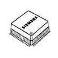
PEB3264H-V1.4 Infineon Technologies, PEB3264H-V1.4 Datasheet - Page 273

PEB3264H-V1.4
Manufacturer Part Number
PEB3264H-V1.4
Description
Manufacturer
Infineon Technologies
Datasheet
1.PEB3264H-V1.4.pdf
(383 pages)
Specifications of PEB3264H-V1.4
On-hook Transmission
Yes
Polarity Reversal
Yes
On-chip Ring Relay Driver
Yes
Operating Temp Range
-40C to 85C
Operating Temperature Classification
Industrial
Mounting
Surface Mount
Lead Free Status / RoHS Status
Not Compliant
- Current page: 273 of 383
- Download datasheet (6Mb)
Preliminary
Bit
DBL-CLK
X-SLOPE
R-SLOPE
NO-
DRIVE-0
SHIFT
PCMO[2:0] The whole PCM timing is moved by PCMO data periods against the FSC
Data Sheet
05
H
DBL-CLK X-SLOPE R-SLOPE NO-DRIVE-0
PCMC1
7
Clock mode for the PCM interface (see
DBL-CLK = 0
DBL-CLK = 1
Transmit Slope (see
X-SLOPE = 0
X-SLOPE = 1
Receive Slope (see
R-SLOPE = 0
R-SLOPE = 1
Driving Mode for Bit 0 (only available in single-clocking mode).
NO-DRIVE = 0
NO-DRIVE = 1
Shifts the access edges by one clock cycle in double clocking mode.
SHIFT = 0
SHIFT = 1
signal.
PCMO[2:0] = 0 0 0
PCMO[2:0] = 0 0 1
PCMO[2:0] = 1 1 1
6
PCM Configuration Register 1
SLICOFI-2x Command Structure and Programming
5
Figure 59
Figure 59
Transmission starts with rising edge of the clock.
Transmission starts with falling edge of the clock.
Single clocking is used.
Double clocking is used.
Data is sampled with falling edge of the clock.
Data is sampled with rising edge of the clock.
No shift takes place.
Shift takes place.
Bit 0 is driven the entire clock period.
Bit 0 is driven during the first half of the clock period
only.
No offset is added.
One data period is added.
Seven data periods are added.
273
on
on
4
Page
Page
Figure 59
141).
141).
SHIFT
3
on
00
Page
2
H
PCMO[2:0]
DuSLIC-S/-S2
141).
1
2000-07-14
N
0
Related parts for PEB3264H-V1.4
Image
Part Number
Description
Manufacturer
Datasheet
Request
R

Part Number:
Description:
Manufacturer:
Infineon Technologies AG
Datasheet:

Part Number:
Description:
Manufacturer:
Infineon Technologies AG
Datasheet:

Part Number:
Description:
Manufacturer:
Infineon Technologies AG
Datasheet:

Part Number:
Description:
Manufacturer:
Infineon Technologies AG
Datasheet:

Part Number:
Description:
Manufacturer:
Infineon Technologies AG
Datasheet:

Part Number:
Description:
Manufacturer:
Infineon Technologies AG
Datasheet:

Part Number:
Description:
Manufacturer:
Infineon Technologies AG
Datasheet:

Part Number:
Description:
16-bit microcontroller with 2x2 KByte RAM
Manufacturer:
Infineon Technologies AG
Datasheet:

Part Number:
Description:
NPN silicon RF transistor
Manufacturer:
Infineon Technologies AG
Datasheet:

Part Number:
Description:
NPN silicon RF transistor
Manufacturer:
Infineon Technologies AG
Datasheet:

Part Number:
Description:
NPN silicon RF transistor
Manufacturer:
Infineon Technologies AG
Datasheet:

Part Number:
Description:
NPN silicon RF transistor
Manufacturer:
Infineon Technologies AG
Datasheet:

Part Number:
Description:
Si-MMIC-amplifier in SIEGET 25-technologie
Manufacturer:
Infineon Technologies AG
Datasheet:

Part Number:
Description:
IGBT Power Module
Manufacturer:
Infineon Technologies AG
Datasheet:

Part Number:
Description:
IC for switching-mode power supplies
Manufacturer:
Infineon Technologies AG
Datasheet:


