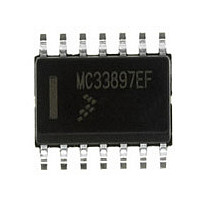
MC33897EF Freescale, MC33897EF Datasheet - Page 14

MC33897EF
Manufacturer Part Number
MC33897EF
Description
Manufacturer
Freescale
Datasheet
1.MC33897EF.pdf
(20 pages)
Specifications of MC33897EF
Number Of Transceivers
1
Power Down Mode
Sleep
Operating Supply Voltage (max)
40V
Package Type
SOIC N
Operating Temperature (max)
125C
Operating Temperature (min)
-40C
Operating Temperature Classification
Automotive
Mounting
Surface Mount
Pin Count
14
Lead Free Status / RoHS Status
Compliant
Available stocks
Company
Part Number
Manufacturer
Quantity
Price
Company:
Part Number:
MC33897EF
Manufacturer:
FREESCALE Semiconductor
Quantity:
20
Part Number:
MC33897EF
Manufacturer:
ON/安森美
Quantity:
20 000
Company:
Part Number:
MC33897EF/R2
Manufacturer:
FREESCAL
Quantity:
34 020
diode is generally used to protect the entire module from
reverse battery and should be selected accordingly.
BUS I /O
(ESD) and /or EMI external circuitry. A set of components is
Timer OSC
internal logic. It is the reference for some of the required
delays.
Timers
active for the required time after the conditions for sleep
mode have been met. It is also used to keep the TXD driver
active for a period of time after it has generated a passive
level on the bus.
Mode Control
operating modes and conditions required for the IC.
BUS RCVR
CMOS level indicating the presence of a logic [0] or a
logic [1]. It also determines the presence of a high-voltage
wake-up (HVWU) signal that is passed to Mode Control and
Timers circuits. An analog filter is used to “de-glitch” the high-
voltage wake-up signal and prevent false exits from the sleep
mode.
14
33897/A/B/C/D/T
FUNCTIONAL DESCRIPTION
FUNCTIONAL BLOCK DIAGRAM COMPONENTS
This input / output may require electrostatic discharge
This circuit generates a 500 kHz signal to be used for
This circuit contains the timing logic used to hold the CNTL
This circuit contains the control logic for the various
This circuit translates the levels on the BUS terminal to a
FUNCTIONAL BLOCK DIAGRAM COMPONENTS
shown in the simplified application diagrams on
this datasheet. The value of the capacitor should be adjusted
downward in direct proportion to the added capacitance of
the ESD or EMI circuits. The series resistance of the inductor
should be kept below 3.5
significantly degrading system noise margins.
TXD BUS DRVR
voltage wake-up signals when enabled by the Mode Control
circuit. It can also provide waveshaping for reduced EMI or
not provide it for the higher data rate mode. The actual data
is received on TXD at CMOS logic levels, then translated by
this circuit to the necessary operating voltages.
Undervoltage Detect
proper operation of the part. If a low-voltage condition is
detected, it sends a signal to disable the BUS RCVR and
TXD BUS DRVR circuits. This prevents incorrect data from
being put on the bus or sent to the MCU.
Load Switch
connected to the BUS to be connected to ground. When a
loss of ground is detected, this switch is opened to prevent
the current that would normally be flowing to the ground from
the module from going back through the load resistor and
raising the bus level. The circuit is opened when the voltage
between GND and VBATT becomes too low as would be the
case if module ground were lost.
This circuit drives the BUS. It can drive it with the higher
This circuit monitors internal operating voltage to assure
The LOAD switch provides a path for an external resistor
Analog Integrated Circuit Device Data
to prevent its voltage drop from
Freescale Semiconductor
page 16
of


