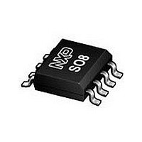
935263363118 NXP Semiconductors, 935263363118 Datasheet - Page 4

935263363118
Manufacturer Part Number
935263363118
Description
Manufacturer
NXP Semiconductors
Datasheet
1.935263363118.pdf
(18 pages)
Specifications of 935263363118
Number Of Transceivers
1
Standard Supported
ISO 11898
Operating Supply Voltage (max)
5.25V
Operating Supply Voltage (typ)
5V
Operating Supply Voltage (min)
4.75V
Package Type
SO
Supply Current
10mA
Operating Temperature (max)
150C
Operating Temperature (min)
-40C
Operating Temperature Classification
Automotive
Mounting
Surface Mount
Pin Count
8
Lead Free Status / RoHS Status
Compliant
Philips Semiconductors
FUNCTIONAL DESCRIPTION
The TJA1050 is the interface between the CAN protocol
controller and the physical bus. It is primarily intended for
high-speed automotive applications using baud rates from
60 kbaud up to 1 Mbaud. It provides differential transmit
capability to the bus and differential receiver capability to
the CAN protocol controller. It is fully compatible to the
“ISO 11898” standard.
A current-limiting circuit protects the transmitter output
stage from damage caused by accidental short-circuit to
either positive or negative supply voltage, although power
dissipation increases during this fault condition.
A thermal protection circuit protects the IC from damage
by switching off the transmitter if the junction temperature
exceeds a value of approximately 165 C. Because the
transmitter dissipates most of the power, the power
dissipation and temperature of the IC is reduced. All other
IC functions continue to operate. The transmitter off-state
resets when pin TXD goes HIGH. The thermal protection
circuit is particularly needed when a bus line short-circuits.
The pins CANH and CANL are protected from automotive
electrical transients (according to “ISO 7637” ; see Fig.4).
Table 1 Function table of the CAN transceiver; X = don’t care
2003 Oct 22
<2 V (not powered)
2 V < V
High speed CAN transceiver
4.75 V to 5.25 V
4.75 V to 5.25 V
4.75 V to 5.25 V
CC
V
CC
< 4.75 V
HIGH (or
floating)
LOW
>2 V
TXD
X
X
LOW (or
floating)
HIGH
S
X
X
X
0 V < V
0 V < V
0.5V
0.5V
CANH
HIGH
4
CANH
CANH
Control pin S allows two operating modes to be selected:
high-speed mode or silent mode.
The high-speed mode is the normal operating mode and is
selected by connecting pin S to ground. It is the default
mode if pin S is not connected. However, to ensure EMI
performance in applications using only the high-speed
mode, it is recommended that pin S is connected to
ground.
In the silent mode, the transmitter is disabled. All other
IC functions continue to operate. The silent mode is
selected by connecting pin S to V
prevent network communication from being blocked, due
to a CAN controller which is out of control.
A ‘TXD dominant time-out’ timer circuit prevents the bus
lines being driven to a permanent dominant state (blocking
all network communication) if pin TXD is forced
permanently LOW by a hardware and/or software
application failure. The timer is triggered by a negative
edge on pin TXD. If the duration of the LOW-level on
pin TXD exceeds the internal timer value, the transmitter is
disabled, driving the bus into a recessive state. The timer
is reset by a positive edge on pin TXD.
CC
CC
< V
< V
CC
CC
0 V < V
0 V < V
0.5V
0.5V
CANL
LOW
CANL
CANL
CC
CC
< V
< V
CC
CC
BUS STATE
CC
recessive
recessive
recessive
recessive
dominant
and can be used to
Product specification
TJA1050
HIGH
HIGH
LOW
RXD
X
X


