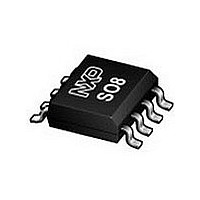
PCA82C251T/N3 NXP Semiconductors, PCA82C251T/N3 Datasheet - Page 6

PCA82C251T/N3
Manufacturer Part Number
PCA82C251T/N3
Description
11N8511
Manufacturer
NXP Semiconductors
Specifications of PCA82C251T/N3
Number Of Transceivers
1
Power Down Mode
Standby
Standard Supported
ISO 11898
Operating Supply Voltage (max)
5.5V
Operating Supply Voltage (typ)
5V
Operating Supply Voltage (min)
4.5V
Package Type
SO
Supply Current
85mA
Operating Temperature (max)
125C
Operating Temperature (min)
-40C
Operating Temperature Classification
Automotive
Mounting
Surface Mount
Pin Count
8
Ic Interface Type
Serial
No. Of Tx Buffers
1
No. Of Rx Buffers
1
Supply Voltage Range
4.5V To 5.5V
Digital Ic Case Style
SOIC
No. Of Pins
8
Operating Temperature Range
-40°C To +125°C
Rohs Compliant
Yes
Lead Free Status / RoHS Status
Compliant
Available stocks
Company
Part Number
Manufacturer
Quantity
Price
Part Number:
PCA82C251T/N3
Manufacturer:
NXP/恩智浦
Quantity:
20 000
Company:
Part Number:
PCA82C251T/N3.118
Manufacturer:
NXP
Quantity:
200 000
Company:
Part Number:
PCA82C251T/N3Ј¬118
Manufacturer:
IEP
Quantity:
5 000
NXP Semiconductors
Table 8.
V
ground (pin 2); positive input current; all parameters are guaranteed over the ambient temperature range by design, but only
100 % tested at +25
[1]
[2]
PCA82C251_4
Product data sheet
Symbol Parameter
V
V
V
R
R
Reference output
V
Timing (R
t
t
t
t
t
t
SR⎪
t
t
Standby/Slope control (pin 8)
V
I
V
bit
onTXD
offTXD
onRXD
offRXD
onRXD
WAKE
dRXDL
slope
CC
diff(hys)
OH
OL
ref
stb
slope
i
diff
= 4.5 V to 5.5 V; T
I
This is valid for the receiver in all modes: High-speed, Slope control and Standby.
1
= I
4
= I
differential input hysteresis
HIGH-level output voltage
LOW-level output voltage
input resistance
differential input resistance
reference output voltage
bit time
delay TXD to bus active
delay TXD to bus inactive
delay TXD to receiver active
delay TXD to receiver inactive
delay TXD to receiver active
CANH, CANL slew rate
wake-up time from Standby
(via pin 8)
bus dominant to RXD LOW
input voltage for Standby mode
Slope control mode current
Slope control mode voltage
L
Characteristics
5
= 60 Ω; C
= 0 mA; 0 V < V
°
C.
L
amb
= 100 Ω; unless otherwise specified; see
=
6
−
…continued
< V
40
CC
°
C to +125
; 0 V < V
7
< V
°
Conditions
see
pin 4; I
pin 4; I
I
CANH, CANL
V
V
minimum; V
V
V
V
R
V
R
R
R
R
R
R
see
V
C; R
4
8
8
8
8
8
CC
8
8
8
8
8
8
8
8
= 10 mA
CC
= 1 V; ⎪I
= 4 V; ⎪I
= 1 V
= 1 V
= 1 V
= 4 V; see
= 0 Ω; T
= 0 Ω; V
= 0 kΩ; T
= 0 kΩ
= 47 kΩ
= 47 kΩ
= 47 kΩ
Figure 5
Figure 7
= 4.5 V to 5.1 V
; V
Rev. 04 — 28 January 2010
L
= 60
4
4
8
= −100 μA
= 1 mA
= V
5
5
amb
CC
CC
Ω
8
⎪ < 50 μA
⎪ < 5 μA
amb
; I
= 1 V
; T
Figure 7
= 4.5 V to 5.1 V
8
< +85 °C
amb
< +85 °C
>
−
< 90 °C.
10
μ
Figure
A; unless otherwise specified; all voltages referenced to
4,
Figure 6
CAN transceiver for 24 V systems
and
5
-
0.4V
Min
-
0.8V
0
0
20
0.45V
0.4V
-
-
-
-
-
-
-
-
-
-
-
-
0.75V
−10
Figure 7
CC
CC
CC
CC
CC
PCA82C251
Typ
150
-
-
-
-
-
-
-
-
-
40
55
80
80
90
90
290
440
7
-
-
-
-
-
© NXP B.V. 2010. All rights reserved.
Max
-
V
0.2V
1.5
25
100
0.55V
0.6V
1
50
80
120
150
170
170
190
400
550
-
20
3
-
−200
0.6V
CC
CC
CC
CC
CC
Unit
mV
V
V
V
kΩ
kΩ
V
V
μs
ns
ns
ns
ns
ns
ns
ns
ns
ns
V/μs
μs
μs
V
μA
V
6 of 16


